

Quantum Interconnects in Silicon-based Photonics
SEP 29, 20259 MIN READ
Generate Your Research Report Instantly with AI Agent
PatSnap Eureka helps you evaluate technical feasibility & market potential.
Quantum Photonics Background and Objectives
Quantum interconnects represent a critical frontier in the evolution of quantum computing and communication systems. The integration of quantum technologies with silicon-based photonics has emerged as a promising approach to address scalability challenges in quantum information processing. This technological convergence builds upon decades of development in classical silicon photonics while incorporating quantum mechanical principles to enable novel functionalities.
The historical trajectory of quantum photonics began with fundamental experiments demonstrating quantum interference and entanglement in the 1980s and 1990s. By the early 2000s, researchers had successfully demonstrated basic quantum operations using photons as qubits. The integration with silicon platforms gained momentum around 2010, leveraging the mature CMOS fabrication infrastructure to potentially enable large-scale quantum photonic circuits.
Silicon-based quantum photonics offers several advantages, including compatibility with existing semiconductor manufacturing processes, potential for high integration density, and operation at telecommunications wavelengths. These characteristics position silicon as an attractive material platform for realizing practical quantum interconnect technologies that can bridge quantum processing nodes.
The primary technical objectives in this field include developing efficient single-photon sources and detectors on silicon platforms, creating low-loss quantum state transfer mechanisms between distant qubits, and establishing protocols for maintaining quantum coherence across integrated photonic networks. Additionally, researchers aim to demonstrate fault-tolerant quantum operations and scalable entanglement distribution using silicon photonic architectures.
Current research trends indicate a growing focus on hybrid approaches that combine the strengths of different material platforms. For instance, integrating III-V semiconductors with silicon to overcome silicon's indirect bandgap limitations for light emission, or incorporating superconducting elements for enhanced detection capabilities. These hybrid systems seek to leverage silicon's manufacturing advantages while compensating for its inherent physical constraints.
The evolution of quantum interconnects in silicon photonics is increasingly driven by practical applications, moving beyond proof-of-concept demonstrations toward systems that can address real-world challenges in quantum computing and secure communications. This includes developing interfaces between different types of quantum systems, such as superconducting qubits and photonic networks, to create comprehensive quantum information processing architectures.
Looking forward, the field is progressing toward quantum advantage demonstrations where silicon-based quantum photonic systems can perform specific tasks more efficiently than classical alternatives. The ultimate goal remains the realization of scalable, fault-tolerant quantum networks that can serve as the foundation for distributed quantum computing and the quantum internet.
Market Analysis for Silicon-based Quantum Interconnects
The global market for silicon-based quantum interconnects is experiencing rapid growth, driven by increasing investments in quantum computing infrastructure and the need for scalable quantum communication networks. Current market estimates value the quantum interconnect segment at approximately $1.2 billion in 2023, with projections indicating a compound annual growth rate of 24% through 2030, potentially reaching $5.7 billion by the end of the decade.
Silicon photonics provides a particularly attractive platform for quantum interconnects due to its compatibility with existing semiconductor manufacturing infrastructure. This compatibility significantly reduces production costs and enables easier integration with classical computing systems. The market for silicon-based quantum interconnects specifically is expected to grow faster than the overall quantum interconnect market, with some industry analysts predicting a 30% CAGR over the next five years.
Key market drivers include the increasing demand for quantum-secure communications in financial services, healthcare, and government sectors. The financial services industry represents the largest current market segment, accounting for approximately 35% of total market demand, primarily for quantum key distribution applications. Defense and intelligence agencies follow closely, representing about 28% of the market.
Geographically, North America leads the market with approximately 42% share, followed by Europe (27%) and Asia-Pacific (24%). China's significant investments in quantum technologies are rapidly expanding the Asia-Pacific market share, with projections suggesting it may overtake Europe by 2026.
The commercial landscape features both established technology corporations and specialized quantum startups. Major semiconductor companies like Intel, IBM, and Global Foundries have dedicated significant R&D resources to silicon-based quantum interconnect technologies. Meanwhile, specialized startups such as PsiQuantum, Xanadu, and Silicon Quantum Computing have attracted substantial venture capital funding, with total investments exceeding $1.5 billion since 2020.
Customer adoption patterns reveal a transition from research-focused applications toward more practical commercial implementations. Early adopters primarily include national laboratories and large technology companies, but financial institutions and telecommunications providers are increasingly deploying pilot projects. Market surveys indicate that 63% of Fortune 500 companies are either implementing or planning to implement quantum-secure communication networks within the next three years.
Supply chain considerations remain a significant factor affecting market growth. The specialized materials and precision manufacturing requirements create potential bottlenecks, particularly for high-purity silicon wafers and specialized photonic components. These supply constraints are expected to partially limit market growth in the near term until manufacturing capacity expands to meet demand.
Technical Challenges in Quantum-Photonic Integration
The integration of quantum systems with silicon photonics presents formidable technical challenges that must be overcome to realize practical quantum interconnects. One of the primary obstacles is maintaining quantum coherence during information transfer between different quantum systems. Quantum states are extremely fragile and susceptible to decoherence from environmental interactions, requiring sophisticated isolation techniques and error correction mechanisms.
Material compatibility issues pose significant barriers to seamless integration. Silicon, while excellent for classical photonics, has inherent limitations for quantum applications due to its indirect bandgap and centro-symmetric crystal structure. These properties make it challenging to generate and manipulate single photons efficiently within the silicon platform, necessitating hybrid approaches that combine silicon with other materials like III-V semiconductors or diamond with nitrogen-vacancy centers.
Fabrication precision requirements for quantum-photonic devices exceed those of classical counterparts by orders of magnitude. Quantum operations demand nanometer-scale precision in waveguide dimensions and surface roughness below 1nm to minimize scattering losses that would destroy quantum information. Current manufacturing processes struggle to consistently achieve these tolerances at scale.
Temperature management presents another critical challenge. Many quantum systems require cryogenic temperatures (often below 4K) to operate effectively, while silicon photonic circuits typically function at room temperature. Creating interfaces between these temperature regimes without introducing thermal noise or mechanical stress requires innovative engineering solutions.
The development of efficient quantum-classical interfaces represents a significant hurdle. These interfaces must translate between classical control signals and quantum information states with minimal loss and decoherence. Current approaches suffer from high insertion losses and limited bandwidth, restricting system performance.
Scalability remains perhaps the most daunting challenge. While laboratory demonstrations have shown promising results for small-scale quantum-photonic components, scaling these systems to thousands or millions of qubits—necessary for practical quantum computing applications—introduces exponential complexity in terms of control systems, error correction, and system integration.
Signal conversion between different quantum information carriers (e.g., from stationary qubits to flying qubits) introduces fidelity losses that accumulate throughout the system. Current conversion efficiencies typically fall below 90%, whereas practical quantum networks require efficiencies exceeding 99% to maintain quantum advantage over classical systems.
Current Silicon-based Quantum Interconnect Architectures
01 Silicon-based quantum photonic integrated circuits
Silicon-based platforms enable the integration of quantum photonic components on a single chip, facilitating quantum information processing. These integrated circuits combine quantum light sources, waveguides, and detectors to create scalable quantum systems. The silicon platform leverages existing semiconductor manufacturing techniques to produce complex quantum photonic circuits with high precision and reproducibility, making it suitable for practical quantum computing applications.- Silicon-based quantum photonic integrated circuits: Silicon-based platforms enable the integration of quantum photonic components on a single chip, facilitating quantum information processing. These integrated circuits combine quantum light sources, waveguides, and detectors to create scalable quantum systems. The silicon platform leverages existing semiconductor manufacturing techniques to produce complex quantum photonic circuits with high precision and reproducibility.
- Quantum interconnect architectures for distributed quantum computing: Specialized interconnect architectures enable the linking of multiple quantum processing units through silicon photonic networks. These architectures facilitate quantum entanglement distribution between physically separated quantum nodes while maintaining quantum coherence. The designs incorporate quantum repeaters, transducers, and routing mechanisms to enable scalable quantum networks for distributed quantum computing applications.
- Silicon-based quantum light sources and single-photon detectors: Integration of quantum light sources and single-photon detectors in silicon photonic platforms enables efficient quantum communication systems. These components utilize silicon's material properties to generate, manipulate, and detect individual photons with high fidelity. Advanced fabrication techniques allow for the creation of quantum emitters and superconducting nanowire single-photon detectors directly on silicon substrates.
- Quantum memory integration with silicon photonics: Quantum memory elements integrated with silicon photonic circuits enable the storage and retrieval of quantum states. These hybrid systems combine the processing capabilities of silicon photonics with specialized materials for quantum state preservation. The integration allows for synchronization of quantum operations and creation of quantum repeater nodes essential for long-distance quantum networks.
- Hybrid quantum-classical interconnect systems: Hybrid architectures combine classical silicon photonic circuitry with quantum components to create practical quantum communication systems. These designs leverage conventional photonic elements for signal routing while preserving quantum information in specialized quantum channels. The approach enables gradual integration of quantum technologies into existing photonic infrastructure while maintaining compatibility with classical communication systems.
02 Quantum entanglement generation and manipulation in silicon photonics
Silicon photonic structures can be designed to generate and manipulate quantum entanglement, a critical resource for quantum communication and computing. These designs incorporate specialized waveguides, resonators, and interferometric structures that enable the creation of entangled photon pairs through nonlinear optical processes. The ability to precisely control quantum states on a silicon platform allows for complex quantum operations while maintaining coherence across interconnected components.Expand Specific Solutions03 Hybrid quantum-classical interconnect technologies
Hybrid approaches combine silicon photonics with other material platforms to overcome limitations in quantum information processing. These interconnect technologies enable the integration of quantum light sources (often made from III-V materials) with silicon waveguides and electronic control circuitry. The hybrid approach allows each component to be optimized separately while maintaining efficient coupling between different subsystems, creating more versatile and functional quantum photonic systems.Expand Specific Solutions04 Quantum memory integration with silicon photonics
Quantum memories are essential components for quantum repeaters and quantum networks, allowing for the temporary storage of quantum information. Silicon-based photonic platforms can be integrated with quantum memory elements, such as color centers, rare-earth doped materials, or atomic ensembles. These integrated memory elements enable synchronization between different parts of a quantum network and facilitate long-distance quantum communication protocols.Expand Specific Solutions05 Scalable quantum interconnect architectures
Scalable architectures for quantum interconnects address the challenges of connecting multiple quantum processing nodes. These designs incorporate low-loss waveguides, efficient couplers, and routing structures that maintain quantum coherence across the network. Silicon photonics enables the development of complex topologies with multiple quantum nodes connected through reconfigurable optical paths, supporting distributed quantum computing and quantum network applications.Expand Specific Solutions
Leading Organizations in Quantum Interconnect Development
Quantum Interconnects in Silicon-based Photonics is currently in an early growth phase, with the market expected to expand significantly as quantum computing advances. The global market is projected to reach several billion dollars by 2030, driven by increasing investments in quantum technologies. Technical maturity varies across implementations, with companies like Intel, PsiQuantum, and Huawei leading commercial development through silicon photonics integration. Academic institutions including MIT, Zhejiang University, and California Institute of Technology are advancing fundamental research. The ecosystem shows a collaborative pattern between semiconductor giants (Intel, STMicroelectronics), specialized quantum startups (PsiQuantum), and research institutions, with integration challenges between quantum systems and conventional silicon photonics remaining a key focus area.
PsiQuantum Corp.
Technical Solution: PsiQuantum has developed a silicon-based photonic quantum computing architecture that addresses quantum interconnect challenges through their unique approach to fault-tolerant quantum computing. Their technology integrates quantum photonic components directly into silicon photonic chips, using standard semiconductor manufacturing processes. The company employs a fusion-based quantum computing model where photonic qubits are manipulated and entangled through specialized optical circuits. Their quantum interconnect solution utilizes waveguides fabricated in silicon to transmit quantum information between different parts of the quantum processor with minimal decoherence. PsiQuantum has partnered with GlobalFoundries to manufacture their silicon photonic chips at scale, demonstrating the industrial viability of their approach. Their quantum interconnect technology enables the creation of large-scale quantum systems by connecting multiple photonic modules through low-loss optical interfaces, addressing one of the key challenges in scaling quantum computers beyond laboratory demonstrations.
Strengths: Leverages existing silicon photonics manufacturing infrastructure, enabling faster scaling and lower production costs. Photonic qubits are less sensitive to thermal noise than solid-state alternatives, allowing operation at higher temperatures. Weaknesses: Photon loss in silicon waveguides remains a challenge for maintaining quantum coherence over longer distances. The technology requires precise optical alignment and packaging solutions that are still being developed.
Massachusetts Institute of Technology
Technical Solution: MIT has developed pioneering quantum interconnect technologies for silicon photonics through their Quantum Photonics Laboratory. Their approach focuses on creating high-fidelity quantum entanglement distribution networks using silicon-based photonic integrated circuits. MIT researchers have demonstrated novel designs for on-chip quantum interference circuits that maintain quantum coherence while manipulating photonic qubits. Their technology incorporates specialized waveguide structures with ultra-low propagation losses to preserve quantum information during transmission. MIT has also developed innovative quantum memory elements integrated into silicon photonic platforms, allowing for temporary storage and synchronization of quantum states. Their quantum interconnect solution includes on-chip quantum frequency conversion modules that enable interfacing between different quantum systems operating at different wavelengths. MIT researchers have demonstrated entanglement distribution between silicon photonic chips using their interconnect technology, achieving high fidelity quantum state transfer. Their recent work includes the development of error correction protocols specifically designed for silicon photonic quantum networks, addressing one of the key challenges in practical quantum communication systems.
Strengths: Cutting-edge research addressing fundamental challenges in quantum coherence preservation in silicon photonics. Their comprehensive approach integrates multiple quantum functionalities (generation, manipulation, detection) on a single platform. Weaknesses: As a research institution, their technologies may be at lower technology readiness levels compared to commercial entities. Some of their advanced designs require specialized fabrication techniques that may be challenging to scale commercially.
Key Patents and Research in Quantum Photonic Interfaces
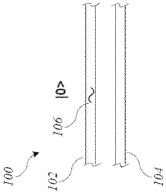
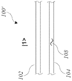
Time bin qubit converter
PatentWO2024054261A2
Innovation
- A system comprising a first photonic integrated circuit with a qubit encoder that converts spatial-mode qubits to temporal-mode qubits using an optical delay and switch, and a second photonic integrated circuit with a qubit decoder that converts them back, utilizing a dual-rail qubit bus with waveguide delay lines and optical switches synchronized with a clock signal.

Quantum Error Correction in Photonic Networks
Quantum Error Correction in Photonic Networks represents a critical frontier in the development of reliable quantum communication systems based on silicon photonics. The inherent fragility of quantum states necessitates robust error correction mechanisms to maintain quantum information integrity across interconnected systems. Current photonic quantum error correction (QEC) protocols primarily employ redundancy-based approaches, where quantum information is encoded across multiple physical qubits to create logical qubits that can withstand certain types of errors.
Surface codes have emerged as particularly promising for photonic networks due to their high error thresholds and compatibility with planar architectures. These codes can be implemented using integrated silicon photonic circuits, where quantum states are encoded in path, polarization, or time-bin degrees of freedom of photons. Recent experimental demonstrations have achieved error correction thresholds approaching 1% in controlled laboratory environments, though practical deployment in real-world networks remains challenging.
The integration of QEC with silicon-based photonic interconnects presents unique opportunities and challenges. Silicon's CMOS compatibility enables the fabrication of complex error correction circuits alongside classical control electronics on the same chip. However, the non-deterministic nature of many quantum photonic operations complicates the implementation of certain QEC protocols that require deterministic gates.
Measurement-based QEC approaches offer a potential solution, as they can leverage the relative ease of performing measurements in photonic systems. These protocols use ancilla photons and feed-forward techniques to detect and correct errors without disrupting the quantum information being processed. Recent demonstrations have shown promising results using silicon ring resonators as quantum memories with integrated error correction capabilities.
Topological quantum error correction represents another frontier, where quantum information is protected by encoding it in non-local degrees of freedom that are inherently resistant to local perturbations. Researchers have proposed implementations using silicon photonic lattice structures that support topologically protected states, though experimental realizations remain limited.
The scalability of QEC in photonic networks faces significant challenges, particularly in terms of resource overhead. Current estimates suggest that thousands of physical qubits may be required for each logical qubit to achieve fault-tolerance. Silicon photonics offers potential advantages through high component density and the possibility of multiplexing techniques to reduce this overhead, but substantial improvements in photon source efficiency, detector performance, and low-loss waveguides are still needed.
International Standards for Quantum Communication Systems
The development of quantum communication systems necessitates robust international standards to ensure interoperability, security, and reliability across different implementations. Currently, several international organizations are actively working on standardizing quantum communication technologies, with the International Telecommunication Union (ITU) and the International Organization for Standardization (ISO) leading these efforts. The ITU-T Study Group 13 has established the Focus Group on Quantum Information Technology for Networks (FG-QIT4N), which is developing frameworks and architectures for quantum key distribution (QKD) networks.
The European Telecommunications Standards Institute (ETSI) has formed the Industry Specification Group on QKD (ISG-QKD), which has published several specifications addressing security proofs, component characterization, and application interfaces. These standards are particularly relevant for silicon-based photonic quantum interconnects, as they define the parameters for optical components used in quantum communication systems.
In Asia, China has been particularly active in quantum standardization, with the Chinese National Institute of Metrology developing measurement standards for single-photon detectors and other quantum components. Japan's National Institute of Information and Communications Technology (NICT) has also contributed significantly to international standardization efforts, particularly in the area of quantum repeaters essential for long-distance quantum networks.
For silicon-based photonic quantum interconnects specifically, the IEEE P1913 working group is developing standards for software-defined quantum communication, which includes specifications for the integration of quantum components with classical photonic circuits. The P1913 standard aims to establish common interfaces between quantum and classical systems, facilitating the development of hybrid quantum-classical networks.
Critical gaps in current standardization efforts include the lack of unified metrics for evaluating quantum interconnect performance, absence of standardized testing procedures for silicon photonic quantum devices, and insufficient protocols for quantum-classical interface management. These gaps present significant challenges for the widespread adoption of quantum communication technologies, particularly in silicon photonics platforms where integration with existing infrastructure is crucial.
Future standardization priorities should focus on developing benchmarks for quantum interconnect efficiency, establishing certification procedures for quantum-secure communication systems, and creating interoperability frameworks for different quantum technologies. Additionally, standards addressing the unique requirements of silicon-based quantum photonics, such as wavelength compatibility with telecom infrastructure and thermal management specifications, will be essential for the commercial deployment of these systems.
Unlock deeper insights with PatSnap Eureka Quick Research — get a full tech report to explore trends and direct your research. Try now!
Generate Your Research Report Instantly with AI Agent
Supercharge your innovation with PatSnap Eureka AI Agent Platform!