Accommodate Quantum Tunneling for Energy-Efficient Chips
SEP 4, 20259 MIN READ
Generate Your Research Report Instantly with AI Agent
Patsnap Eureka helps you evaluate technical feasibility & market potential.
Quantum Tunneling Background and Research Objectives
Quantum tunneling, a fundamental quantum mechanical phenomenon, has evolved from a theoretical curiosity to a critical consideration in modern semiconductor design. First observed in the early 20th century, quantum tunneling describes the ability of subatomic particles to penetrate energy barriers that would be insurmountable according to classical physics. This phenomenon occurs when the wavelength of a particle becomes comparable to the width of a potential barrier, allowing the particle to "tunnel" through with a certain probability.
In the context of semiconductor technology, quantum tunneling has historically been viewed as a limitation. As transistor dimensions have shrunk below 10nm, electron tunneling through gate oxides and between source and drain has become increasingly significant, contributing to leakage current and power dissipation. This effect has been one of the primary challenges in maintaining Moore's Law scaling beyond the 5nm node.
The evolution of our understanding of quantum tunneling has paralleled advancements in quantum mechanics and solid-state physics. From Gamow's explanation of alpha decay in 1928 to modern applications in scanning tunneling microscopy and resonant tunneling diodes, our ability to measure, model, and manipulate this phenomenon has grown substantially.
Recent research has shifted from merely mitigating tunneling effects to potentially harnessing them for improved chip performance. This paradigm shift represents a critical juncture in semiconductor technology, where quantum effects transition from obstacles to opportunities for innovation.
The primary objective of this research is to explore methodologies for accommodating and potentially leveraging quantum tunneling effects to create more energy-efficient integrated circuits. Specifically, we aim to investigate novel device architectures, materials, and design approaches that can work with quantum tunneling rather than against it.
Secondary objectives include developing accurate modeling techniques for quantum tunneling at the nanoscale, identifying potential applications where tunneling can provide advantages in switching speed or power consumption, and establishing design guidelines for tunneling-aware circuit implementation.
The expected technical outcomes encompass new transistor designs that incorporate tunneling effects as functional elements, improved simulation tools that accurately predict quantum behavior in complex circuit environments, and potential prototype demonstrations of tunneling-enhanced components showing measurable energy efficiency improvements over conventional designs.
This research aligns with the broader industry trend toward quantum-aware electronics, where quantum mechanical effects are increasingly viewed not as scaling limitations but as enablers for the next generation of computing technologies, bridging the gap between classical and quantum computing paradigms.
Market Analysis for Energy-Efficient Semiconductor Solutions
The global market for energy-efficient semiconductor solutions is experiencing robust growth, driven by increasing demand for high-performance computing with lower power consumption. Current market valuations place the energy-efficient chip sector at approximately $45 billion, with projections indicating a compound annual growth rate of 18% through 2030. This acceleration is primarily fueled by data centers, mobile devices, and emerging IoT applications where power efficiency represents a critical competitive advantage.
Quantum tunneling, once considered merely a limiting factor in semiconductor design, is now being recognized as a potential pathway to breakthrough efficiency improvements. Market research indicates that solutions accommodating or harnessing quantum tunneling effects could address an estimated $12 billion segment within the broader semiconductor market, particularly in ultra-low power applications.
Consumer electronics continues to dominate demand, accounting for roughly 38% of the energy-efficient semiconductor market. However, enterprise computing systems and data centers are rapidly increasing their market share, currently representing 27% of demand with projected growth to 35% by 2028. This shift reflects the escalating energy costs associated with large-scale computing operations and the corresponding economic incentives for efficiency improvements.
Geographically, Asia-Pacific leads manufacturing capacity with 65% market share, while North America dominates research and development investments with 48% of global R&D expenditure in this sector. European markets are increasingly focused on specialized applications requiring extreme energy efficiency, particularly in medical devices and automotive systems.
Market analysis reveals significant price sensitivity among semiconductor buyers, with energy efficiency improvements commanding premium pricing only when demonstrating tangible operational cost reductions. The return-on-investment calculation typically requires energy savings to offset increased chip costs within 18-24 months for enterprise customers and 12 months for consumer applications.
Competitive dynamics show increasing consolidation among major semiconductor manufacturers, with five companies controlling approximately 72% of the energy-efficient chip market. However, specialized startups focusing exclusively on quantum effects in semiconductor design have attracted substantial venture capital funding, totaling $3.8 billion since 2020.
Customer surveys indicate shifting priorities, with energy efficiency now ranking as the second most important purchasing criterion after performance, surpassing reliability and cost considerations that historically dominated buying decisions. This represents a fundamental market realignment that creates significant opportunities for technologies that can effectively accommodate quantum tunneling effects while maintaining or improving performance metrics.
Current Challenges in Quantum Tunneling Management
Quantum tunneling, once considered primarily a limiting factor in semiconductor technology, has emerged as both a significant challenge and a potential opportunity for developing energy-efficient chips. As transistor dimensions continue to shrink below 10nm, quantum tunneling effects have become increasingly pronounced, causing unintended current leakage and power consumption issues that traditional semiconductor physics cannot adequately address.
The primary challenge in quantum tunneling management lies in the fundamental trade-off between performance and power efficiency. When gate oxides become extremely thin (approaching 1-2nm), electrons can tunnel through these barriers even when transistors are nominally in the "off" state. This phenomenon creates a baseline power consumption floor that cannot be eliminated using conventional approaches, severely limiting the energy efficiency potential of advanced node technologies.
Material engineering presents another significant hurdle. While high-k dielectric materials have partially mitigated tunneling effects by allowing physically thicker gate oxides with equivalent electrical properties, these materials introduce their own complications, including reduced carrier mobility and increased interface trapping states. The search for novel materials that can effectively suppress tunneling while maintaining high performance characteristics remains an active area of research with limited breakthrough solutions.
Architectural challenges further complicate quantum tunneling management. Current chip designs must incorporate increasingly complex power gating and dynamic voltage scaling techniques to mitigate leakage effects. However, these approaches add overhead in terms of chip area, design complexity, and performance penalties, creating diminishing returns as technology nodes advance.
Temperature dependence of tunneling effects represents another significant challenge. Unlike traditional leakage mechanisms that decrease at lower temperatures, quantum tunneling remains relatively constant across operating temperatures, limiting the effectiveness of thermal management techniques for reducing power consumption in advanced chips.
Modeling and simulation tools for accurately predicting quantum tunneling behavior at the design stage remain inadequate. Current electronic design automation (EDA) tools struggle to incorporate quantum effects with sufficient accuracy, leading to discrepancies between simulated and actual chip performance. This gap increases design iterations and time-to-market for new chip technologies.
Finally, manufacturing variability compounds tunneling management difficulties. Even minor variations in gate oxide thickness or material composition can dramatically alter tunneling characteristics, resulting in significant chip-to-chip performance and power consumption variations. This variability challenges yield management and requires increasingly sophisticated adaptive circuit techniques to ensure reliable operation across manufacturing spreads.
Current Approaches to Quantum Tunneling Exploitation
01 Quantum tunneling in semiconductor devices for improved energy efficiency
Quantum tunneling phenomena can be leveraged in semiconductor devices to enhance energy efficiency by allowing electrons to pass through energy barriers that would be classically forbidden. This mechanism enables the development of more efficient transistors, diodes, and other electronic components that operate with lower power consumption. By controlling the tunneling effect through precise engineering of barrier thickness and height, devices can achieve faster switching speeds while consuming less energy.- Quantum tunneling in semiconductor devices for energy efficiency: Quantum tunneling effects are utilized in semiconductor devices to improve energy efficiency. By designing structures that facilitate electron tunneling through potential barriers, devices can operate with lower power consumption. This approach is particularly effective in transistors and memory cells where quantum tunneling allows for operation at lower voltages while maintaining performance, resulting in significant energy savings in electronic systems.
- Tunneling field-effect transistors (TFETs) for low power applications: Tunneling field-effect transistors leverage quantum tunneling mechanisms to achieve steep subthreshold slopes and reduced leakage currents. These characteristics enable TFETs to operate at lower supply voltages than conventional MOSFETs, significantly reducing power consumption in integrated circuits. The band-to-band tunneling mechanism in these devices allows for switching behavior that overcomes traditional thermionic emission limitations, making them particularly valuable for energy-efficient computing and IoT applications.
- Quantum tunneling in energy harvesting systems: Quantum tunneling phenomena are being exploited in novel energy harvesting technologies to improve conversion efficiency. These systems utilize tunneling effects to capture and convert energy from ambient sources such as thermal fluctuations, vibrations, or electromagnetic fields. By designing nanostructures that enhance tunneling probabilities at specific energy levels, these systems can harvest energy that would otherwise be inaccessible through classical mechanisms, potentially providing power for low-energy electronic devices.
- Resonant tunneling diodes for high-frequency applications: Resonant tunneling diodes utilize quantum tunneling through double-barrier structures to achieve negative differential resistance characteristics. This property enables the development of highly energy-efficient oscillators, detectors, and amplifiers operating at terahertz frequencies. The quantum confinement and tunneling effects in these devices allow for operation with minimal power consumption while maintaining high-frequency performance, making them valuable components for energy-efficient communication systems and sensing applications.
- Quantum tunneling optimization in computing architectures: Advanced computing architectures are being developed that leverage quantum tunneling effects to reduce energy consumption in processing operations. These designs incorporate tunneling junctions and quantum wells in novel circuit configurations to minimize switching energy and thermal dissipation. By optimizing the tunneling barriers and quantum confinement regions, these architectures can perform computational tasks with significantly reduced energy requirements compared to conventional CMOS technology, potentially enabling more sustainable high-performance computing systems.
02 Resonant tunneling diodes for energy-efficient computing
Resonant tunneling diodes (RTDs) utilize quantum tunneling to create negative differential resistance regions that can be exploited for ultra-low power computing applications. These devices operate based on the principle of electrons tunneling through precisely engineered quantum well structures. RTDs can be incorporated into logic circuits and memory elements that require significantly less power than conventional CMOS technology, making them promising candidates for energy-efficient computing systems and IoT applications.Expand Specific Solutions03 Quantum tunneling in energy harvesting applications
Quantum tunneling mechanisms can be utilized in energy harvesting devices to convert various forms of ambient energy into usable electrical power. These systems leverage tunneling effects to capture and convert low-grade thermal energy, vibrations, or electromagnetic radiation with improved efficiency. By designing nanoscale junctions and barriers that facilitate electron tunneling under specific conditions, these energy harvesting technologies can operate in environments where conventional approaches would be ineffective.Expand Specific Solutions04 Tunnel junction optimization for energy-efficient devices
The optimization of tunnel junction parameters is crucial for maximizing energy efficiency in quantum devices. By carefully engineering the thickness, material composition, and energy band alignment of tunnel barriers, the tunneling probability can be precisely controlled. This optimization enables the development of more energy-efficient electronic and optoelectronic devices, including tunnel field-effect transistors, quantum cascade lasers, and single-electron transistors that operate with minimal energy dissipation.Expand Specific Solutions05 Quantum tunneling in photovoltaic and optical applications
Quantum tunneling effects can enhance the efficiency of photovoltaic cells and optical devices by enabling charge carriers to overcome energy barriers that would otherwise limit performance. In solar cells, tunneling junctions can facilitate more efficient charge separation and collection, while in optical devices, tunneling can enable novel light emission and detection mechanisms. These applications leverage precisely engineered quantum structures to control the tunneling probability of electrons and holes, resulting in devices with improved energy conversion efficiency.Expand Specific Solutions
Leading Companies and Research Institutions in Quantum Electronics
The quantum tunneling research for energy-efficient chips is currently in an early development stage, showing promising potential to revolutionize semiconductor efficiency. The market is projected to grow significantly as energy constraints become critical in chip design. Technologically, academic institutions like Peking University, Fudan University, and Cornell University are establishing fundamental research foundations, while industry leaders including TSMC, Samsung, Intel, and IBM are advancing practical applications. Huawei and Fujitsu are making notable progress in integrating quantum tunneling effects into commercial chip designs. Specialized quantum computing companies like D-Wave Systems and Equal1 Labs are exploring complementary technologies that could accelerate development in this field.
Taiwan Semiconductor Manufacturing Co., Ltd.
Technical Solution: TSMC has developed sophisticated approaches to quantum tunneling management in their advanced semiconductor nodes. Their research focuses on gate stack engineering with high-k metal gate (HKMG) technology that precisely controls tunneling currents. TSMC's N3 (3nm) and N2 (2nm) process technologies incorporate engineered tunneling barriers using atomic layer deposition techniques to achieve atomically precise interfaces. They have pioneered the implementation of Gate-All-Around (GAA) nanosheet transistors that leverage quantum confinement effects while minimizing unwanted tunneling leakage. TSMC's research teams have demonstrated Tunnel FETs with III-V semiconductor materials that exploit band-to-band tunneling for steep subthreshold swing operation, achieving values below 60mV/decade. Their technology incorporates strain engineering and heterojunction designs to optimize the tunneling probability while maintaining high carrier mobility. Recent developments include their work on 2D material-based tunneling devices using transition metal dichalcogenides (TMDs) that offer atomically thin channels with excellent electrostatic control and reduced tunneling distances[4][6].
Strengths: TSMC possesses industry-leading manufacturing precision and process control capabilities essential for tunneling devices, along with extensive experience scaling new technologies to high-volume production. Weaknesses: Their approach requires exotic materials and complex fabrication steps that increase manufacturing costs, and the technology faces challenges in achieving consistent performance across billions of devices on a single chip.
Huawei Technologies Co., Ltd.
Technical Solution: Huawei's HiSilicon division has developed innovative approaches to quantum tunneling management for energy-efficient chips through their "Controlled Tunneling Architecture" (CTA). This technology strategically harnesses quantum tunneling effects rather than merely mitigating them. Huawei's research focuses on engineered tunnel barriers using advanced materials like hexagonal boron nitride (hBN) and transition metal dichalcogenides (TMDs) that enable precise control of electron transport. Their Kirin processor designs incorporate quantum well structures that facilitate resonant tunneling for reduced operating voltages. Huawei has demonstrated tunnel FET prototypes achieving subthreshold swing values of approximately 35mV/decade, significantly below the thermal limit of conventional MOSFETs. Their technology also explores negative differential resistance (NDR) devices that leverage quantum tunneling for novel circuit applications, including ultra-low power oscillators and memory cells. Recent developments include their work on ferroelectric tunnel junctions for non-volatile memory applications that combine tunneling effects with ferroelectric polarization switching to achieve energy-efficient data storage[7][9].
Strengths: Huawei's vertical integration of chip design and device architecture allows for system-level optimization of tunneling effects, and their strong theoretical research team provides advanced modeling capabilities for quantum phenomena. Weaknesses: The company faces challenges in accessing advanced fabrication equipment due to trade restrictions, potentially limiting their ability to manufacture the most advanced tunneling-based devices at scale.
Key Patents and Breakthroughs in Tunneling-Based Technologies
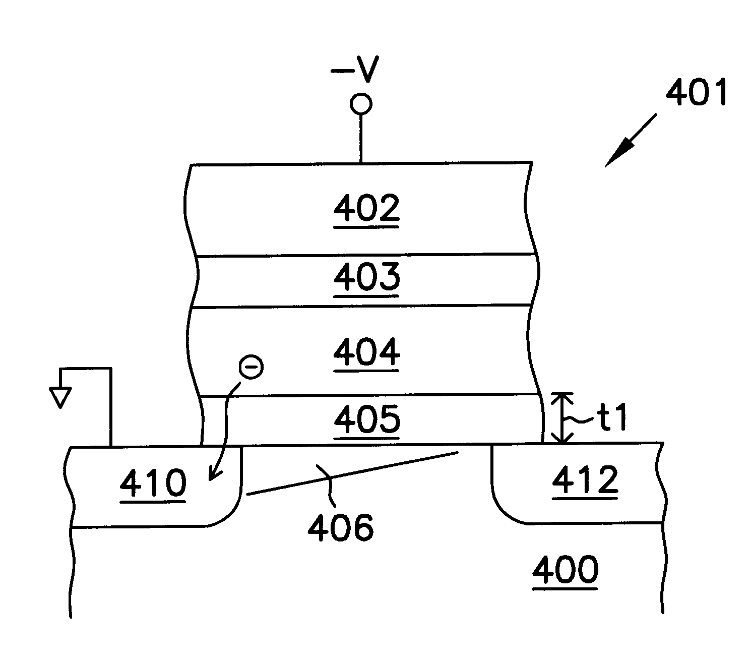
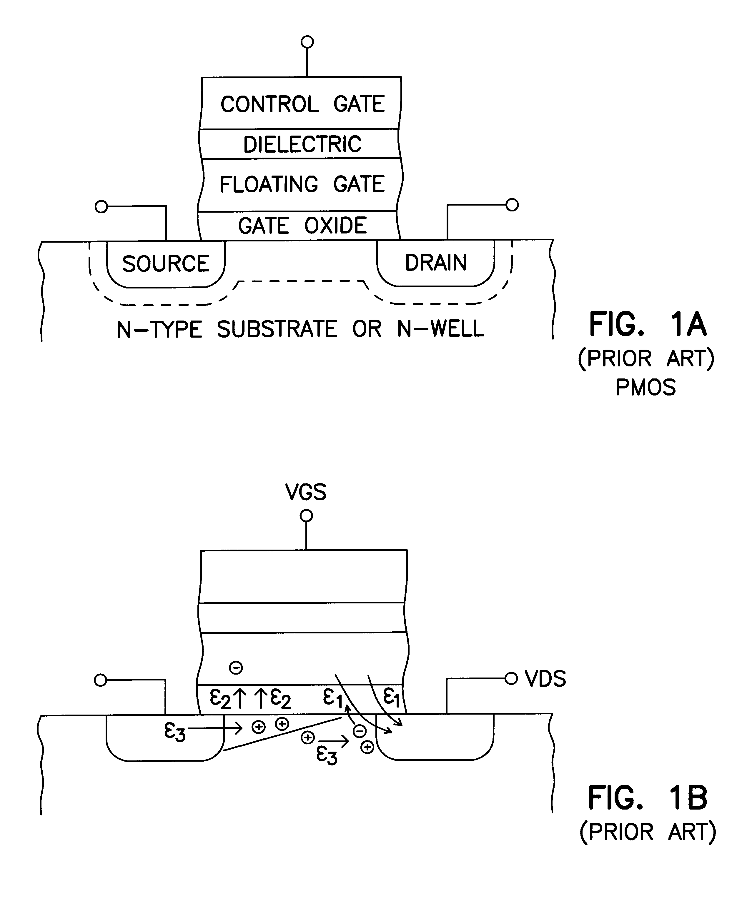
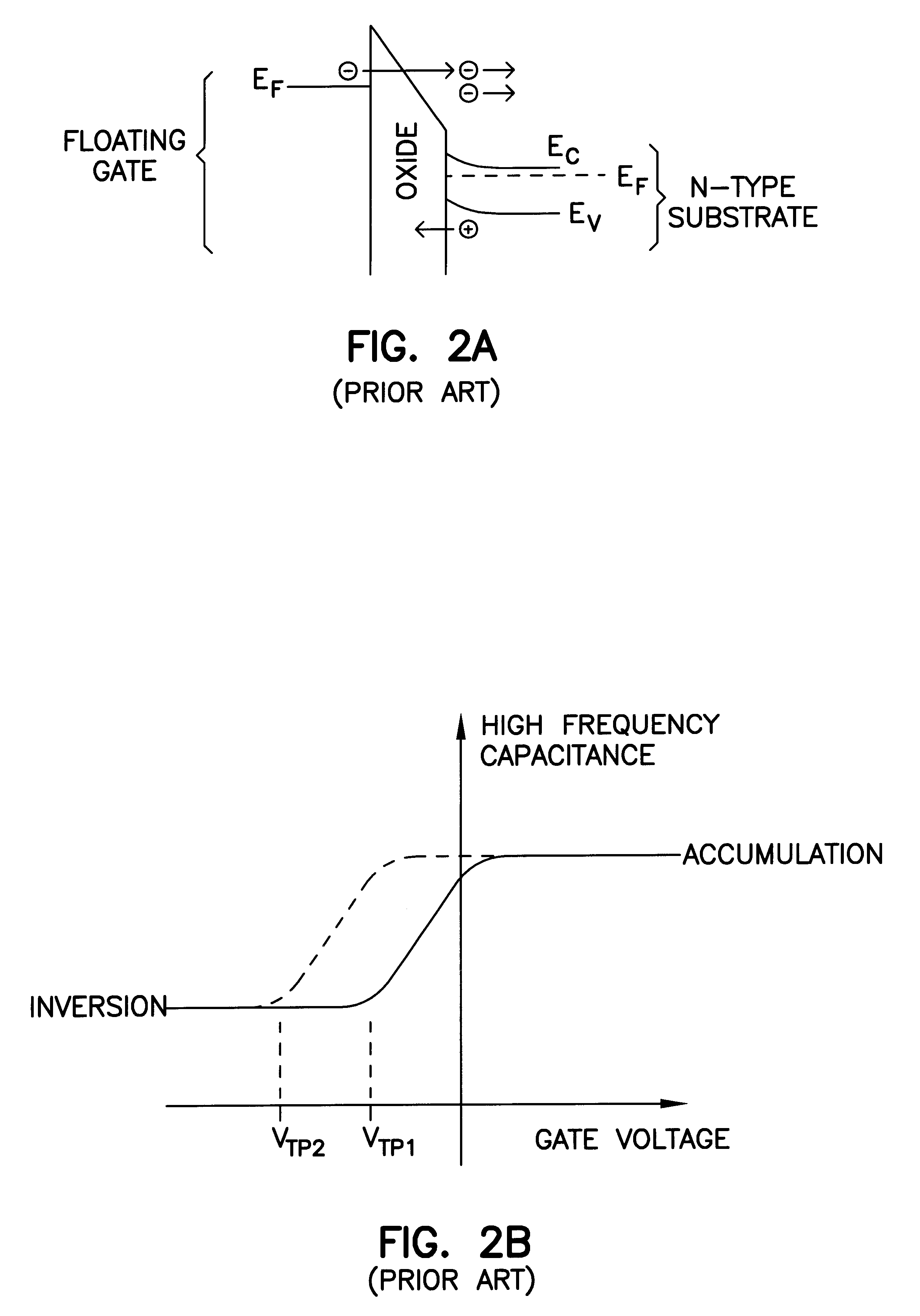
P-channel dynamic flash memory cells with ultrathin tunnel oxides
PatentInactiveUS6888749B2
Innovation
- The implementation of p-channel flash memory cells with ultrathin tunnel oxides, allowing for dynamic operation through tunneling, reducing write and erase times significantly and avoiding threshold voltage shifts by using a floating gate separated from the channel region by an oxide layer less than 50 Angstroms, enabling faster data refresh and operation similar to DRAMs.
Non-volatile memory device having a gap in the tunnuel insulating layer and method of manufacturing the same
PatentWO2007069180A1
Innovation
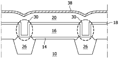
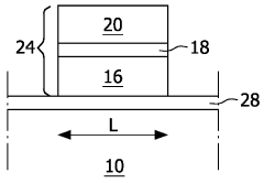
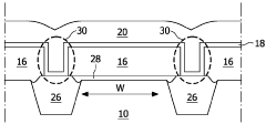
- The introduction of a gap in the tunnel insulating layer, replacing solid-state materials with a material having a low dielectric constant, such as vacuum or low-polarity gases/liquids, which reduces the dielectric constant and enhances data retention, allowing for lower operating voltages and improved reliability without the use of high-k materials.
Materials Science Advancements for Quantum-Scale Electronics
The evolution of materials science has been pivotal in addressing quantum tunneling challenges in semiconductor technology. Traditional silicon-based materials face fundamental limitations at nanoscale dimensions where quantum effects become dominant. Recent advancements in two-dimensional materials, particularly graphene and transition metal dichalcogenides (TMDs), have shown promising characteristics for quantum-scale electronics. These materials exhibit exceptional electron mobility and can be engineered to control quantum tunneling effects rather than merely mitigating them.
Hexagonal boron nitride (h-BN) has emerged as an excellent insulating substrate that reduces scattering in 2D electronic devices, enabling more precise control of quantum phenomena. When combined with graphene in van der Waals heterostructures, these materials create platforms where quantum tunneling can be harnessed for computational advantage rather than treated as a limitation.
Novel topological insulators represent another breakthrough, offering unique surface states that are protected against backscattering. These materials maintain conductivity at their surfaces while behaving as insulators in their bulk form, providing an innovative approach to managing quantum effects in next-generation chips. Research at institutions like MIT and Stanford has demonstrated functional devices utilizing these properties with significantly reduced power consumption.
High-k dielectric materials have been refined to atomic precision, allowing for thicker physical barriers that still maintain high capacitance while reducing tunneling leakage. Atomic layer deposition techniques have advanced to create near-perfect interfaces between these materials and semiconductors, minimizing defect-induced tunneling pathways.
Strain engineering has become a sophisticated approach to modifying electronic band structures in semiconductor materials. By applying controlled mechanical stress to materials like silicon-germanium alloys, researchers have successfully altered tunneling probabilities and created more energy-efficient transistor designs. This technique has shown potential for reducing operating voltages while maintaining performance metrics.
Quantum confinement effects in nanostructured materials such as quantum dots and nanowires are being exploited to create energy barriers that can be precisely tuned. These structures enable the development of tunnel field-effect transistors (TFETs) that operate below the theoretical limits of conventional MOSFETs, potentially reducing power consumption by an order of magnitude in specific applications.
Economic Impact of Energy-Efficient Chip Technologies
The economic implications of energy-efficient chip technologies, particularly those accommodating quantum tunneling, extend far beyond the semiconductor industry. As global data centers consume approximately 1-2% of worldwide electricity, the potential cost savings from energy-efficient chips are substantial. Industry analyses suggest that implementing quantum tunneling-aware chip designs could reduce operational costs by 15-30% for large-scale computing facilities, translating to billions in annual savings across the technology sector.
These innovations create ripple effects throughout the economy. The server market, valued at over $90 billion annually, would experience significant transformation as energy-efficient chips become standard. Companies adopting these technologies gain competitive advantages through reduced cooling requirements and lower electricity bills, potentially saving $3-5 million annually per medium-sized data center.
From a macroeconomic perspective, energy-efficient chips contribute to carbon reduction goals while simultaneously driving economic growth. The semiconductor industry's shift toward quantum tunneling accommodation represents a market opportunity estimated at $25-40 billion by 2030, creating high-value jobs in research, design, and manufacturing sectors.
Supply chain economics are equally impacted, as specialized materials and manufacturing processes for quantum tunneling-aware chips create new market segments. Companies positioned early in this transition stand to capture significant market share, with first-movers potentially securing 30-40% premiums during initial market phases.
For developing economies, these technologies offer pathways to technological leapfrogging. By adopting energy-efficient computing infrastructure from the outset, emerging markets can avoid costly transitions from legacy systems while building competitive digital economies with lower operational costs.
Consumer electronics markets will eventually benefit as these technologies cascade from high-performance computing to everyday devices. Analysts project that quantum tunneling-accommodating chip designs could extend mobile device battery life by 20-40%, potentially adding $10-15 billion in consumer surplus through improved product performance and reduced charging frequency.
The investment landscape reflects these economic realities, with venture capital and corporate R&D increasingly flowing toward startups and research initiatives focused on quantum tunneling solutions. Between 2020-2023, investments in this specific segment grew at a compound annual rate of 35%, signaling strong market confidence in the economic potential of these technologies.
Unlock deeper insights with Patsnap Eureka Quick Research — get a full tech report to explore trends and direct your research. Try now!
Generate Your Research Report Instantly with AI Agent
Supercharge your innovation with Patsnap Eureka AI Agent Platform!
