

Debugging Transverse Waveforms in Electronic Diagnostics
JUL 29, 20259 MIN READ
Generate Your Research Report Instantly with AI Agent
PatSnap Eureka helps you evaluate technical feasibility & market potential.
Transverse Waveform Debugging Background and Objectives
Transverse waveform debugging in electronic diagnostics has emerged as a critical area of research in recent years, driven by the increasing complexity of electronic systems and the need for more precise diagnostic tools. This field has evolved from simple oscilloscope-based measurements to sophisticated signal analysis techniques that can detect and isolate minute anomalies in complex waveforms.
The development of transverse waveform debugging techniques can be traced back to the early days of electronic engineering, where basic time-domain analysis was the primary method for signal characterization. As electronic systems became more intricate, the limitations of traditional debugging methods became apparent, necessitating the development of more advanced techniques.
The current technological landscape demands highly accurate and efficient diagnostic tools capable of analyzing transverse waveforms in real-time. This need is particularly pronounced in industries such as telecommunications, aerospace, and high-performance computing, where signal integrity is paramount. The ability to quickly identify and rectify waveform anomalies can significantly reduce downtime and improve overall system reliability.
One of the primary objectives of research in this field is to enhance the resolution and accuracy of transverse waveform analysis. This involves developing new algorithms and hardware solutions that can detect subtle variations in signal characteristics, such as jitter, crosstalk, and impedance mismatches. Additionally, there is a growing focus on integrating machine learning and artificial intelligence techniques to automate the debugging process and provide more insightful diagnostics.
Another key goal is to improve the scalability of transverse waveform debugging techniques. As electronic systems continue to grow in complexity, with higher data rates and more intricate interconnects, diagnostic tools must evolve to handle these challenges. This includes developing methods for simultaneous multi-channel analysis and techniques for correlating waveform anomalies across different parts of a system.
Researchers are also exploring ways to make transverse waveform debugging more accessible and user-friendly. This involves creating intuitive interfaces and visualization tools that can present complex waveform data in a more understandable format. The aim is to bridge the gap between expert-level analysis and practical, on-the-field diagnostics, enabling a wider range of engineers and technicians to effectively troubleshoot electronic systems.
As we look to the future, the field of transverse waveform debugging is expected to play an increasingly important role in ensuring the reliability and performance of next-generation electronic systems. The ongoing research in this area promises to yield new insights and tools that will shape the landscape of electronic diagnostics for years to come.
Electronic Diagnostics Market Analysis
The electronic diagnostics market has experienced significant growth in recent years, driven by the increasing complexity of electronic systems and the growing demand for efficient troubleshooting tools. This market encompasses a wide range of diagnostic equipment, including oscilloscopes, logic analyzers, and specialized software for debugging transverse waveforms. The global electronic diagnostics market was valued at approximately $7.2 billion in 2020 and is projected to reach $10.5 billion by 2025, growing at a CAGR of 7.8% during the forecast period.
The demand for electronic diagnostic tools is primarily fueled by the rapid advancements in the automotive, aerospace, and consumer electronics industries. These sectors require sophisticated diagnostic equipment to ensure the reliability and performance of their increasingly complex electronic systems. The automotive industry, in particular, has been a major driver of growth in the electronic diagnostics market, as modern vehicles incorporate an ever-increasing number of electronic components and systems.
In the context of debugging transverse waveforms, there is a growing need for specialized diagnostic tools that can accurately analyze and interpret complex signal patterns. This demand is particularly strong in industries such as telecommunications, where high-speed data transmission requires precise waveform analysis to maintain signal integrity and minimize errors.
The market for electronic diagnostics is characterized by intense competition among key players, including Keysight Technologies, Tektronix, Rohde & Schwarz, and National Instruments. These companies are continuously innovating to develop more advanced diagnostic tools that can handle the increasing complexity of electronic systems and provide more accurate and efficient debugging capabilities for transverse waveforms.
Geographically, North America and Europe currently dominate the electronic diagnostics market, accounting for approximately 60% of the global market share. However, the Asia-Pacific region is expected to witness the highest growth rate in the coming years, driven by the rapid industrialization and technological advancements in countries like China, Japan, and South Korea.
The COVID-19 pandemic has had a mixed impact on the electronic diagnostics market. While it initially caused disruptions in the supply chain and reduced demand from certain industries, it has also accelerated the adoption of remote diagnostic tools and virtual testing solutions. This shift towards remote diagnostics is expected to continue even after the pandemic, creating new opportunities for market growth and innovation in the field of electronic diagnostics, particularly in the area of transverse waveform debugging.
Current Challenges in Transverse Waveform Debugging
Transverse waveform debugging in electronic diagnostics faces several significant challenges that hinder its effectiveness and reliability. One of the primary obstacles is the complexity of modern electronic systems, which often involve multiple layers of interconnected components and intricate signal pathways. This complexity makes it difficult to isolate and identify the source of waveform distortions or anomalies.
The high-speed nature of many electronic systems presents another major challenge. As clock speeds and data rates continue to increase, the time window for accurate waveform analysis becomes increasingly narrow. This requires more sophisticated and precise measurement techniques, as well as advanced signal processing algorithms to capture and interpret transient events accurately.
Signal integrity issues pose a significant hurdle in transverse waveform debugging. Factors such as crosstalk, electromagnetic interference, and impedance mismatches can introduce noise and distortions that mask or alter the true waveform characteristics. Distinguishing between genuine signal anomalies and artifacts introduced by the measurement process itself becomes a critical challenge.
The limitations of current debugging tools and equipment also contribute to the difficulties in transverse waveform analysis. Many oscilloscopes and logic analyzers struggle to provide the necessary bandwidth, sample rate, and resolution required for high-fidelity waveform capture in advanced electronic systems. This can lead to aliasing, missed events, or inaccurate representations of the actual signal behavior.
Another challenge lies in the interpretation of complex waveforms, particularly in mixed-signal environments where analog and digital signals coexist. Engineers must possess a deep understanding of both domains to accurately diagnose issues and correlate waveform anomalies with specific circuit behaviors or design flaws.
The increasing prevalence of embedded systems and system-on-chip (SoC) designs introduces additional complications. These highly integrated architectures often have limited access points for probing and measurement, making it challenging to obtain comprehensive waveform data from internal nodes without disrupting normal operation.
Furthermore, the dynamic nature of many electronic systems, such as those employing adaptive algorithms or variable clock rates, adds another layer of complexity to waveform debugging. Capturing and analyzing transient events or intermittent faults in these systems requires sophisticated triggering mechanisms and long-term data acquisition capabilities that push the limits of current debugging technologies.
Existing Transverse Waveform Debugging Solutions
01 Waveform analysis and debugging techniques
Advanced techniques for analyzing and debugging transverse waveforms in electronic systems. These methods involve sophisticated signal processing algorithms and visualization tools to identify and resolve issues in complex waveform patterns.- Waveform analysis and debugging techniques: Advanced techniques for analyzing and debugging transverse waveforms in electronic systems. These methods involve sophisticated signal processing algorithms and visualization tools to identify and resolve issues in complex waveform patterns.
- Automated debugging systems for waveform analysis: Automated systems designed to streamline the debugging process for transverse waveforms. These systems employ machine learning and artificial intelligence to detect anomalies, predict potential issues, and suggest corrective actions.
- Hardware-software co-debugging for waveform issues: Integrated approaches that combine hardware and software debugging techniques for addressing transverse waveform problems. These methods provide a comprehensive solution for identifying and resolving issues that span both hardware and software domains.
- Real-time waveform monitoring and debugging: Systems and methods for real-time monitoring and debugging of transverse waveforms. These solutions enable immediate detection and resolution of waveform anomalies, reducing downtime and improving system reliability.
- Simulation-based waveform debugging techniques: Advanced simulation techniques for debugging transverse waveforms in complex electronic systems. These methods allow engineers to model and analyze waveform behavior in virtual environments, facilitating efficient problem identification and resolution before physical implementation.
02 Hardware-based debugging solutions
Implementation of hardware-specific debugging solutions for transverse waveforms. This includes specialized circuits and components designed to capture, analyze, and troubleshoot waveform anomalies in real-time hardware environments.Expand Specific Solutions03 Software-based debugging tools
Development of software tools and applications specifically designed for debugging transverse waveforms. These tools offer features such as waveform simulation, error detection algorithms, and interactive debugging interfaces to assist in identifying and resolving waveform-related issues.Expand Specific Solutions04 Integration of machine learning in waveform debugging
Application of machine learning techniques to enhance the debugging process for transverse waveforms. This involves using AI algorithms to analyze patterns, predict potential issues, and suggest optimized solutions for complex waveform problems.Expand Specific Solutions05 Cross-platform waveform debugging frameworks
Development of versatile debugging frameworks that can be applied across different platforms and systems for transverse waveform analysis. These frameworks provide a standardized approach to waveform debugging, enabling efficient troubleshooting across various hardware and software environments.Expand Specific Solutions
Key Players in Electronic Diagnostics Industry
The research on debugging transverse waveforms in electronic diagnostics is in a developing stage, with a growing market driven by increasing demand for advanced diagnostic tools. The technology's maturity varies among key players, with established companies like Koninklijke Philips NV, FUJIFILM Corp., and Medtronic, Inc. leading in innovation. Emerging players such as EMTensor GmbH and Neuroenhancement Lab LLC are introducing novel approaches, while research institutions like MIT and Sunnybrook Research Institute contribute to fundamental advancements. The competitive landscape is diverse, encompassing medical technology giants, specialized diagnostic equipment manufacturers, and academic institutions, indicating a dynamic and evolving field with significant potential for growth and technological breakthroughs.
Massachusetts Institute of Technology
Technical Solution: MIT has developed advanced techniques for debugging transverse waveforms in electronic diagnostics. Their approach utilizes high-speed digital oscilloscopes with bandwidths exceeding 100 GHz to capture and analyze ultra-fast transient signals[1]. They have also implemented advanced signal processing algorithms, including wavelet transforms and machine learning-based pattern recognition, to identify and characterize anomalies in complex waveforms[2]. MIT's research includes the development of on-chip probing techniques that allow for non-invasive measurement of high-frequency signals directly on integrated circuits[3].
Strengths: Cutting-edge research capabilities, access to state-of-the-art equipment, and interdisciplinary collaboration. Weaknesses: High cost of implementation and potential complexity for practical industrial applications.
Anritsu Corp.
Technical Solution: Anritsu Corporation has developed specialized Vector Network Analyzers (VNAs) and Signal Quality Analyzers (SQAs) for debugging transverse waveforms in electronic diagnostics. Their VNA-based approach allows for precise characterization of high-speed digital signals, including eye diagram analysis and jitter measurements[4]. Anritsu's SQAs incorporate advanced error detection and correction algorithms, enabling real-time analysis of complex modulation schemes used in modern communication systems[5]. They have also introduced innovative software tools for automated waveform analysis and fault diagnosis in electronic systems[6].
Strengths: Extensive experience in test and measurement equipment, strong focus on high-speed digital and RF applications. Weaknesses: Solutions may be less adaptable to non-communications related electronic diagnostics.
Core Innovations in Waveform Analysis
Biomedical signal denoising techniques
PatentInactiveEP1613209A1
Innovation
- The use of wavelet transformations with different thresholds for various scales to decompose and denoise electrograms, setting insignificant noise-related coefficients to zero while preserving significant information, which can be implemented in medical devices with limited computational resources.
Systems and methods for improving identification of issues associated with detecting anomalous conditions
PatentActiveUS11994543B2
Innovation
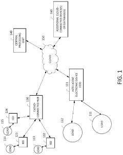
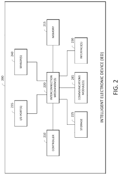
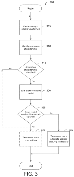
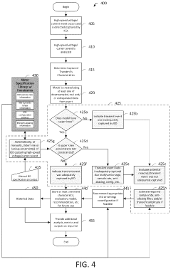
- A method and system that automatically identify metering constraints of IEDs by capturing energy-related waveforms, processing electrical measurement data to detect anomalous characteristics, and building an event constraint model to determine if the waveforms are adequately captured, with the option to adjust settings or replace devices to improve capturing inadequacies.
Signal Integrity and EMC Considerations
Signal integrity and electromagnetic compatibility (EMC) are critical considerations in the research on debugging transverse waveforms in electronic diagnostics. These factors significantly impact the accuracy and reliability of diagnostic measurements, especially when dealing with high-speed digital signals and sensitive analog circuits.
In terms of signal integrity, transverse waveforms are particularly susceptible to distortions caused by impedance mismatches, crosstalk, and reflections. These issues can lead to false readings and misinterpretation of diagnostic data. To address these challenges, researchers must implement proper impedance matching techniques, such as controlled impedance traces and termination resistors. Additionally, careful routing of signal paths and the use of differential signaling can help minimize crosstalk and maintain signal fidelity.
EMC considerations are equally important in electronic diagnostics, as electromagnetic interference (EMI) can severely degrade the quality of transverse waveform measurements. Shielding techniques, including the use of ground planes and EMI suppression materials, play a crucial role in protecting sensitive diagnostic circuits from external noise sources. Furthermore, proper grounding and power distribution network (PDN) design are essential to minimize common-mode noise and ensure clean power delivery to the diagnostic components.
Advanced PCB layout techniques, such as guard traces and split planes, can be employed to isolate critical signal paths and reduce the coupling of noise between different circuit sections. These techniques are particularly valuable when dealing with mixed-signal designs, where high-frequency digital circuits coexist with sensitive analog components.
The selection of appropriate connectors and cabling is another vital aspect of maintaining signal integrity and EMC in electronic diagnostic systems. High-quality, shielded cables and connectors with controlled impedance characteristics help preserve signal quality and minimize EMI ingress and egress.
To effectively debug transverse waveforms, researchers must also consider the impact of measurement equipment on signal integrity. High-bandwidth oscilloscopes and probes with low capacitance and inductance are essential for accurately capturing fast-edge transients and high-frequency components of the waveforms. Proper probe compensation and de-embedding techniques should be applied to remove the effects of measurement fixtures and probes from the acquired data.
In conclusion, addressing signal integrity and EMC challenges is paramount in the research on debugging transverse waveforms in electronic diagnostics. By implementing robust design practices and leveraging advanced measurement techniques, researchers can significantly improve the accuracy and reliability of their diagnostic systems, ultimately leading to more effective troubleshooting and analysis of complex electronic circuits.
Automated Debugging Tools and AI Integration
The integration of automated debugging tools and artificial intelligence (AI) has revolutionized the process of debugging transverse waveforms in electronic diagnostics. These advanced technologies have significantly enhanced the efficiency and accuracy of identifying and resolving issues in complex electronic systems.
Automated debugging tools have evolved to incorporate sophisticated algorithms capable of analyzing vast amounts of data from transverse waveforms. These tools can quickly detect anomalies, patterns, and potential sources of errors that may not be immediately apparent to human operators. By automating the initial stages of the debugging process, engineers can focus their efforts on more complex problem-solving tasks.
AI integration has further enhanced the capabilities of automated debugging tools. Machine learning algorithms can be trained on large datasets of known waveform issues, enabling them to recognize and classify new problems with high accuracy. This predictive capability allows for faster identification of root causes and more targeted troubleshooting approaches.
Deep learning techniques, such as convolutional neural networks (CNNs), have shown particular promise in analyzing transverse waveforms. CNNs can effectively process and interpret the spatial and temporal characteristics of waveforms, identifying subtle patterns and correlations that may elude traditional analysis methods. This has led to improved diagnostic accuracy and reduced false positives in electronic systems.
Natural language processing (NLP) has also been incorporated into debugging tools, allowing engineers to interact with the system using natural language queries. This feature enables more intuitive exploration of waveform data and facilitates easier collaboration among team members working on complex debugging tasks.
Real-time monitoring and adaptive learning capabilities have become integral components of AI-enhanced debugging tools. These systems can continuously analyze incoming waveform data, adjusting their parameters and detection thresholds based on new information. This dynamic approach ensures that the debugging process remains effective even as electronic systems evolve or encounter novel issues.
The integration of AI and automated debugging tools has also led to the development of predictive maintenance capabilities. By analyzing historical waveform data and system performance metrics, these tools can forecast potential failures or degradation in electronic components before they occur. This proactive approach helps minimize downtime and optimize maintenance schedules in critical electronic systems.
As AI and automated debugging technologies continue to advance, we can expect even more sophisticated tools that combine multiple AI techniques, such as reinforcement learning and generative adversarial networks, to tackle increasingly complex debugging scenarios in electronic diagnostics. These developments promise to further streamline the debugging process, reduce human error, and enhance the overall reliability of electronic systems across various industries.
Unlock deeper insights with PatSnap Eureka Quick Research — get a full tech report to explore trends and direct your research. Try now!
Generate Your Research Report Instantly with AI Agent
Supercharge your innovation with PatSnap Eureka AI Agent Platform!