The Optimization of Transverse Waves in Fluidic Lab on Chip Devices
JUL 29, 20259 MIN READ
Generate Your Research Report Instantly with AI Agent
Patsnap Eureka helps you evaluate technical feasibility & market potential.
Transverse Wave Fundamentals and Objectives
Transverse waves have emerged as a critical component in the development of fluidic lab-on-chip devices, offering unique capabilities for manipulating and analyzing microscale fluid dynamics. These waves, characterized by oscillations perpendicular to the direction of wave propagation, have garnered significant attention in the microfluidics community due to their potential to enhance mixing, separation, and detection processes at the microscale level.
The evolution of transverse wave technology in lab-on-chip devices can be traced back to the early 2000s when researchers began exploring novel methods to overcome the limitations of laminar flow in microfluidic channels. As the field progressed, the integration of acoustic and electromagnetic transducers enabled the generation of controlled transverse waves within these miniaturized systems, opening up new possibilities for fluid manipulation and analysis.
The primary objective of optimizing transverse waves in fluidic lab-on-chip devices is to enhance the overall performance and functionality of these systems. This includes improving mixing efficiency in microchannels, increasing the sensitivity and specificity of detection methods, and developing more precise particle manipulation techniques. By fine-tuning the frequency, amplitude, and spatial distribution of transverse waves, researchers aim to achieve unprecedented control over fluid behavior at the microscale.
One of the key challenges in this field is the complex interplay between transverse waves and the fluid properties within the confined geometries of lab-on-chip devices. Understanding and modeling these interactions require a multidisciplinary approach, combining principles from fluid dynamics, acoustics, and electromagnetic theory. As such, the optimization of transverse waves necessitates a deep understanding of the underlying physical phenomena and their practical implications in microfluidic systems.
Recent advancements in transverse wave technology have led to the development of novel applications in areas such as point-of-care diagnostics, drug discovery, and environmental monitoring. These innovations have demonstrated the potential of transverse waves to revolutionize traditional laboratory processes by enabling rapid, efficient, and highly sensitive analyses on miniaturized platforms.
Looking ahead, the field of transverse wave optimization in fluidic lab-on-chip devices is poised for continued growth and innovation. Emerging research directions include the exploration of higher-frequency waves for enhanced spatial resolution, the integration of multiple wave types for synergistic effects, and the development of adaptive wave generation systems that can respond to real-time feedback from the fluid environment.
Market Analysis for Fluidic LOC Devices
The market for fluidic Lab on Chip (LOC) devices has been experiencing significant growth in recent years, driven by the increasing demand for point-of-care diagnostics, personalized medicine, and miniaturized analytical systems. The global market for microfluidic devices, which includes LOC systems, is projected to reach substantial value in the coming years, with a compound annual growth rate (CAGR) exceeding industry averages.
The healthcare sector remains the primary driver of market demand for fluidic LOC devices. The ability to perform complex analytical tasks with minimal sample volumes and rapid turnaround times has made these devices particularly attractive for applications such as disease diagnosis, drug discovery, and genomic analysis. The ongoing COVID-19 pandemic has further accelerated the adoption of LOC technologies for rapid testing and diagnostics.
Beyond healthcare, the market for fluidic LOC devices is expanding into other sectors. Environmental monitoring, food safety testing, and chemical analysis industries are increasingly recognizing the benefits of miniaturized, portable analytical systems. This diversification of applications is expected to contribute significantly to market growth in the coming years.
Geographically, North America and Europe currently dominate the market for fluidic LOC devices, owing to their advanced healthcare infrastructure and substantial research and development investments. However, the Asia-Pacific region is emerging as a rapidly growing market, driven by increasing healthcare expenditure, rising awareness of personalized medicine, and government initiatives to promote biotechnology research.
The market landscape is characterized by a mix of established players and innovative startups. Major companies in the field are focusing on developing integrated systems that combine microfluidic chips with detection and analysis capabilities. Concurrently, numerous startups are entering the market with novel technologies and applications, contributing to a dynamic and competitive environment.
Key market trends include the integration of advanced materials and fabrication techniques to enhance device performance and reduce costs. Additionally, there is a growing emphasis on developing user-friendly, plug-and-play systems that can be operated by non-specialists, expanding the potential user base for these devices.
Challenges in the market include the need for standardization of microfluidic technologies and regulatory hurdles, particularly for medical applications. However, ongoing collaborations between industry, academia, and regulatory bodies are addressing these issues, paving the way for broader market acceptance and adoption of fluidic LOC devices.
Current Challenges in Transverse Wave Implementation
The implementation of transverse waves in fluidic lab on chip devices faces several significant challenges that hinder their widespread adoption and optimization. One of the primary obstacles is the difficulty in generating and controlling precise, localized transverse waves within microfluidic channels. The small scale of these devices makes it challenging to create consistent and reproducible wave patterns without disturbing the overall fluid flow or damaging delicate biological samples.
Another major challenge lies in the integration of wave-generating components into the miniaturized lab on chip systems. Traditional methods of wave generation often involve bulky external equipment, which contradicts the goal of creating compact, portable devices. Researchers are struggling to develop efficient, miniaturized actuators that can produce the required transverse waves without compromising the device's size or functionality.
The interaction between transverse waves and complex fluid dynamics within microfluidic channels presents another significant hurdle. The behavior of fluids at the microscale can be unpredictable, and the introduction of transverse waves further complicates these dynamics. Understanding and modeling these interactions accurately is crucial for optimizing wave-based applications but remains a complex task that requires advanced computational methods and experimental validation.
Energy efficiency is also a critical concern in the implementation of transverse waves. Generating and maintaining these waves often requires a substantial amount of energy, which can lead to localized heating and potential damage to sensitive biological samples. Developing energy-efficient methods for wave generation and propagation is essential for the practical application of this technology in lab on chip devices.
Furthermore, the materials used in the construction of microfluidic devices pose limitations on the effectiveness of transverse waves. Many common materials used in these devices have properties that can dampen or distort wave propagation, reducing the overall efficiency of wave-based operations. Identifying and developing new materials that are compatible with both the microfluidic environment and efficient wave transmission is an ongoing challenge.
Lastly, the scalability of transverse wave implementations across different types and sizes of lab on chip devices remains a significant obstacle. What works effectively in one device configuration may not translate well to others, making it difficult to establish standardized protocols or design principles. This lack of scalability hampers the broader adoption of transverse wave technology in diverse microfluidic applications.
Existing Transverse Wave Optimization Techniques
01 Optimization of transverse wave propagation in optical systems
This approach focuses on improving the propagation of transverse waves in optical systems. It involves techniques for enhancing wave transmission, reducing distortion, and optimizing the overall performance of optical devices that utilize transverse waves. Methods may include advanced waveguide designs, novel material compositions, or innovative structural configurations to achieve better wave control and efficiency.- Optimization of transverse wave generation in piezoelectric devices: Techniques for optimizing the generation of transverse waves in piezoelectric devices, including improved electrode configurations and material selection. These methods enhance the efficiency and precision of transverse wave production for various applications such as sensors and actuators.
- Transverse wave measurement and analysis techniques: Advanced methods for measuring and analyzing transverse waves, including novel sensor designs and signal processing algorithms. These techniques improve the accuracy of wave detection and characterization in fields such as seismology, acoustics, and materials science.
- Transverse wave propagation in optical systems: Optimization strategies for transverse wave propagation in optical systems, focusing on waveguide design, material selection, and signal modulation techniques. These advancements enhance the performance of optical communication systems and photonic devices.
- Transverse wave applications in energy harvesting: Innovative approaches to harnessing transverse waves for energy harvesting applications, including the development of efficient conversion mechanisms and optimized structural designs. These techniques aim to improve the capture and utilization of ambient vibrational energy.
- Transverse wave control in acoustic systems: Methods for optimizing the control and manipulation of transverse waves in acoustic systems, including advanced filtering techniques, wave steering, and noise cancellation. These innovations enhance the performance of audio equipment, ultrasonic devices, and acoustic imaging systems.
02 Transverse wave optimization in acoustic applications
This category deals with optimizing transverse waves in acoustic systems. It encompasses methods for enhancing sound quality, improving signal processing, and increasing the efficiency of acoustic devices. Techniques may involve advanced transducer designs, innovative acoustic materials, or sophisticated signal processing algorithms to achieve better acoustic performance and control of transverse waves.Expand Specific Solutions03 Transverse wave optimization in seismic exploration
This approach focuses on optimizing transverse waves for seismic exploration applications. It includes methods for improving data acquisition, processing, and interpretation of seismic signals. Techniques may involve advanced sensor designs, innovative data processing algorithms, or novel survey methodologies to enhance the accuracy and resolution of subsurface imaging using transverse waves.Expand Specific Solutions04 Optimization of transverse waves in electromagnetic applications
This category deals with optimizing transverse waves in electromagnetic systems. It encompasses methods for improving signal transmission, reducing interference, and enhancing the overall performance of devices that utilize electromagnetic waves. Techniques may include advanced antenna designs, novel materials for wave manipulation, or innovative circuit configurations to achieve better control and efficiency of transverse electromagnetic waves.Expand Specific Solutions05 Transverse wave optimization in quantum systems
This approach focuses on optimizing transverse waves in quantum systems and applications. It involves techniques for enhancing quantum state manipulation, improving quantum information processing, and optimizing the performance of quantum devices that utilize transverse waves. Methods may include advanced quantum circuit designs, novel quantum materials, or innovative quantum control techniques to achieve better quantum coherence and entanglement using transverse waves.Expand Specific Solutions
Key Players in Fluidic LOC Industry
The optimization of transverse waves in fluidic lab-on-chip devices is an emerging field in the early stages of development, with a growing market driven by the increasing demand for miniaturized and efficient diagnostic tools. The technology's maturity is still evolving, with key players like IBM, Hitachi, and Agilent Technologies leading research efforts. Academic institutions such as Purdue University and Ghent University are also contributing significantly to advancements in this area. The market size is expected to expand as the technology finds applications in healthcare, environmental monitoring, and pharmaceutical research. However, challenges in scalability and integration with existing systems remain, indicating that further research and development are necessary to fully realize the potential of this technology.
International Business Machines Corp.
Technical Solution: IBM has developed cutting-edge solutions for optimizing transverse waves in fluidic lab-on-chip devices, leveraging their expertise in microelectronics and nanofabrication. Their approach focuses on integrating advanced acoustic wave generators with sophisticated microfluidic channel designs. IBM has implemented high-frequency, low-power surface acoustic wave (SAW) devices using novel piezoelectric thin films, which allow for precise control of fluid flow and particle manipulation at the microscale[11]. The company has also explored the use of artificial intelligence and machine learning algorithms to optimize the design and operation of these acoustic-based lab-on-chip devices, enhancing their efficiency and adaptability[12]. Additionally, IBM has developed innovative packaging solutions that enable seamless integration of their acoustic wave technology with other lab-on-chip components, facilitating the creation of comprehensive and compact analytical systems.
Strengths: Advanced integration with microelectronics, AI-driven optimization, compact and efficient designs. Weaknesses: Potentially high initial development costs, may require specialized manufacturing processes.
Ghent University
Technical Solution: Ghent University has made significant advancements in the optimization of transverse waves for fluidic lab-on-chip devices. Their research focuses on developing novel acoustic wave generation and manipulation techniques for microfluidic applications. The university has pioneered the use of phononic crystals and acoustic metamaterials to control and shape acoustic waves within microfluidic channels[9]. They have also developed innovative designs for surface acoustic wave (SAW) devices that can generate complex wave patterns, allowing for sophisticated fluid and particle manipulation[10]. Ghent University's approach includes the integration of multiple acoustic wave sources to create dynamic and reconfigurable acoustic fields within lab-on-chip devices. This enables adaptive control of fluid flow and particle positioning, which is crucial for advanced biomedical and chemical analysis applications.
Strengths: Advanced wave shaping capabilities, adaptable and reconfigurable systems. Weaknesses: Complexity in device fabrication, potential challenges in scaling up for mass production.
Innovative Approaches in Wave Manipulation
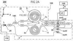
On-chip opto-acoustic interferometers
PatentWO2025014369A1
Innovation
- The integration of primary and auxiliary photonic waveguides with curved trajectories on a membrane, extending over zones with opposite sign expansion/contraction, allowing for increased sensitivity and higher resonance frequencies, and the use of anisotropic pre-stress or crystalline anisotropy to optimize waveguide positioning and resonance modes.
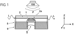
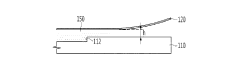
Lab-on-chip and method of driving the same
PatentInactiveJP2011128141A
Innovation
- A lab-on-chip design with adjustable gaps between substrates using a gap adjustment member and pressure application mechanism to control fluid flow and enhance reaction opportunities, incorporating flexible substrates and wedge-shaped gap adjustment for precise control.

Microfluidic Device Fabrication Methods
Microfluidic device fabrication methods have evolved significantly over the past few decades, enabling the development of sophisticated lab-on-chip devices capable of manipulating transverse waves in fluidic environments. The primary fabrication techniques can be broadly categorized into three main approaches: photolithography-based methods, soft lithography, and advanced 3D printing technologies.
Photolithography, a cornerstone technique in microfluidic device fabrication, involves the transfer of geometric patterns from a photomask to a light-sensitive photoresist on a substrate. This process typically utilizes silicon or glass substrates and allows for the creation of highly precise microstructures. The photoresist is then developed, and the exposed areas are etched to create the desired microfluidic channels and features. This method offers excellent resolution and reproducibility, making it ideal for creating complex microfluidic structures necessary for optimizing transverse wave propagation.
Soft lithography, pioneered by George Whitesides and colleagues, has revolutionized microfluidic device fabrication due to its simplicity and cost-effectiveness. This technique primarily uses polydimethylsiloxane (PDMS), a flexible, transparent elastomer, to replicate microstructures from a master mold. The master mold, often created through photolithography, is used to cast PDMS, which is then cured and peeled off to create the microfluidic device. Soft lithography's versatility allows for rapid prototyping and iterative design improvements, crucial for optimizing transverse wave behavior in fluidic lab-on-chip devices.
Advanced 3D printing technologies have recently emerged as promising alternatives for microfluidic device fabrication. Techniques such as stereolithography (SLA), two-photon polymerization (2PP), and digital light processing (DLP) offer unprecedented freedom in designing complex 3D microstructures. These methods enable the creation of intricate channel geometries and integrated components that can significantly enhance the control and manipulation of transverse waves within the device. The ability to rapidly prototype and iterate designs makes 3D printing particularly valuable for research and development in this field.
Each fabrication method presents unique advantages and limitations in the context of optimizing transverse waves in fluidic lab-on-chip devices. Photolithography offers high precision but can be costly and time-consuming for iterative design processes. Soft lithography provides excellent flexibility and cost-effectiveness but may have limitations in creating high-aspect-ratio structures. 3D printing technologies offer unparalleled design freedom but may face challenges in achieving the same level of resolution as traditional photolithography techniques.
The choice of fabrication method often depends on the specific requirements of the transverse wave optimization problem, including the desired channel geometries, material properties, and the need for integrated functionalities. Researchers and engineers must carefully consider these factors when selecting the most appropriate fabrication technique for their specific application in fluidic lab-on-chip devices.
Biosafety Considerations in LOC Applications
Biosafety considerations play a crucial role in the development and implementation of Lab on Chip (LOC) devices, particularly those utilizing transverse waves in fluidic systems. As these miniaturized platforms handle biological samples and potentially hazardous materials, it is imperative to address safety concerns to protect both users and the environment.
One of the primary biosafety considerations in LOC applications is the containment of biological materials. Transverse waves in fluidic systems can potentially generate aerosols or droplets, which may pose risks of sample contamination or exposure to harmful agents. To mitigate these risks, LOC devices must incorporate robust sealing mechanisms and utilize materials resistant to chemical and biological degradation. Additionally, the integration of filtration systems or enclosed chambers can help prevent the release of potentially hazardous particles.
The choice of materials used in LOC fabrication is another critical aspect of biosafety. Materials must be biocompatible, non-toxic, and resistant to chemical reactions that could compromise the integrity of the device or the safety of the samples. Furthermore, the materials should be amenable to sterilization techniques to ensure a contamination-free environment for sensitive biological assays.
Proper disposal protocols for used LOC devices and waste materials are essential to maintain biosafety standards. As these devices may contain biological or chemical residues, they must be treated as biohazardous waste and disposed of according to established guidelines. Implementing clear labeling systems and providing user training on proper handling and disposal procedures are crucial steps in ensuring biosafety compliance.
The optimization of transverse waves in fluidic LOC devices must also consider the potential impact on cellular structures and biomolecules. While these waves can enhance mixing and separation processes, excessive energy levels may lead to cell lysis or protein denaturation. Careful calibration and control of wave parameters are necessary to maintain sample integrity and prevent unintended biological effects.
Biosafety considerations extend to the design of LOC interfaces and user interaction points. Minimizing direct contact with samples and incorporating fail-safe mechanisms can reduce the risk of accidental exposure. Additionally, the integration of real-time monitoring systems for detecting potential leaks or contamination can enhance the overall safety profile of LOC devices.
As LOC technologies continue to advance, it is crucial to stay abreast of evolving biosafety regulations and standards. Regular risk assessments and validation studies should be conducted to ensure that LOC devices meet or exceed current safety requirements. Collaboration with biosafety experts and regulatory bodies can help inform the development of robust safety protocols tailored to the unique challenges posed by transverse wave-based fluidic LOC systems.
Unlock deeper insights with Patsnap Eureka Quick Research — get a full tech report to explore trends and direct your research. Try now!
Generate Your Research Report Instantly with AI Agent
Supercharge your innovation with Patsnap Eureka AI Agent Platform!