Navigate Quantum Tunneling Impact on Low-Power Devices
SEP 4, 20259 MIN READ
Generate Your Research Report Instantly with AI Agent
Patsnap Eureka helps you evaluate technical feasibility & market potential.
Quantum Tunneling Background and Research Objectives
Quantum tunneling represents a fundamental quantum mechanical phenomenon where particles penetrate through energy barriers that would be insurmountable according to classical physics. This effect, first observed in the early 20th century, has evolved from a theoretical curiosity to a critical consideration in modern semiconductor device design. The phenomenon occurs when the wave function of a particle extends beyond a potential barrier, allowing the particle to appear on the opposite side without possessing sufficient energy to overcome the barrier classically.
In the context of low-power electronic devices, quantum tunneling has transformed from being merely a limiting factor to becoming both a challenge and an opportunity. Historically, as device dimensions shrank below 100nm, tunneling effects began to significantly impact device performance, particularly manifesting as leakage currents that increase power consumption in the off-state of transistors.
The evolution of this field has been marked by several key milestones: from the initial theoretical formulations by Gamow and Gurney in the 1920s, to the practical observations in solid-state devices in the 1950s, and finally to the deliberate engineering of tunneling effects in modern devices such as tunnel field-effect transistors (TFETs) and resonant tunneling diodes (RTDs).
Current technological trends indicate a growing importance of quantum tunneling as devices continue to miniaturize toward the physical limits of scaling. With conventional CMOS technology approaching fundamental barriers, understanding and controlling tunneling phenomena has become essential for further advancements in low-power electronics.
The primary objectives of this research are threefold. First, to comprehensively analyze the impact of quantum tunneling on power consumption in sub-10nm semiconductor devices, quantifying both detrimental effects (unwanted leakage) and beneficial applications (tunneling-based switches). Second, to evaluate existing mitigation strategies and their effectiveness across different device architectures and materials. Third, to explore novel approaches that might transform tunneling from a limitation into an advantage for next-generation low-power computing.
This research aims to bridge the gap between theoretical quantum mechanics and practical device engineering, providing actionable insights for semiconductor manufacturers facing tunneling-related challenges. By establishing a clear understanding of tunneling mechanisms in contemporary and emerging device technologies, we seek to contribute to the development of more energy-efficient electronic systems that can support the growing demands of mobile computing, IoT applications, and sustainable computing infrastructure.
Market Analysis for Low-Power Device Technologies
The low-power device market has experienced significant growth over the past decade, driven primarily by the proliferation of mobile devices, Internet of Things (IoT) applications, and wearable technology. This market segment is projected to reach $78.5 billion by 2026, with a compound annual growth rate of 7.9% from 2021 to 2026. The increasing demand for extended battery life and energy-efficient operation across consumer electronics, healthcare devices, and industrial applications continues to fuel this expansion.
Quantum tunneling, once considered merely a limiting factor in semiconductor miniaturization, is now emerging as a critical consideration in the design and optimization of low-power devices. As transistor dimensions approach sub-5nm nodes, quantum effects become increasingly dominant in device behavior. Market research indicates that approximately 35% of semiconductor companies are actively investing in research related to quantum effects management, with quantum tunneling receiving particular attention due to its direct impact on power consumption.
The healthcare wearables segment represents one of the fastest-growing markets for low-power devices, with 23% annual growth. These devices require exceptional power efficiency to maintain continuous monitoring capabilities while minimizing battery replacement. Quantum tunneling optimization could potentially extend battery life by 30-40% in these applications, creating significant competitive advantages for manufacturers who successfully implement such technologies.
Industrial IoT applications constitute another substantial market segment, valued at $12.3 billion in 2021. These applications often deploy sensors in remote or hazardous environments where power availability is limited and maintenance access is challenging. The ability to reduce power consumption through quantum tunneling management could dramatically improve deployment feasibility and operational costs in this sector.
Consumer electronics manufacturers are increasingly marketing power efficiency as a key differentiator. Market surveys indicate that 68% of smartphone users consider battery life a critical factor in purchasing decisions. This consumer preference has intensified competition among device manufacturers to implement advanced power-saving technologies, including those addressing quantum tunneling effects.
Regional analysis shows Asia-Pacific leading the low-power device market with 42% market share, followed by North America (27%) and Europe (21%). China and Taiwan have established dominant positions in manufacturing, while research initiatives addressing quantum effects in semiconductors are concentrated in the United States, Japan, South Korea, and several European countries, particularly Germany and the Netherlands.
The market is witnessing increased collaboration between academic institutions and industry players, with joint research initiatives focusing on quantum tunneling management increasing by 45% since 2018. This trend reflects the recognition that addressing quantum effects requires multidisciplinary expertise spanning quantum physics, materials science, and electrical engineering.
Current Challenges in Quantum Tunneling Management
Quantum tunneling presents significant challenges for modern low-power device development, particularly as semiconductor technology approaches sub-10nm nodes. The fundamental quantum mechanical phenomenon, where electrons penetrate energy barriers they classically shouldn't overcome, creates increasingly problematic leakage currents that undermine power efficiency goals. This effect becomes exponentially more pronounced as device dimensions shrink, creating a fundamental physical limit that threatens continued scaling according to Moore's Law.
Device engineers face the complex challenge of balancing performance requirements with tunneling-induced power leakage. As gate oxides become thinner to maintain electrostatic control, direct tunneling through these barriers increases exponentially. Similarly, drain-induced barrier lowering (DIBL) exacerbates tunneling effects in short-channel devices, creating a difficult optimization problem where improving one parameter often worsens another.
Material selection presents another significant challenge. While high-k dielectrics have helped mitigate gate leakage, their implementation introduces interface quality issues that can degrade carrier mobility. The industry continues to search for novel material combinations that can simultaneously address tunneling concerns while maintaining other essential device characteristics.
Modeling and simulation tools struggle to accurately predict quantum tunneling effects at scale. Current computational approaches often rely on simplifications that fail to capture the full complexity of quantum behavior in realistic device geometries. This creates a disconnect between design expectations and manufactured device performance, leading to costly iteration cycles and suboptimal designs.
Temperature dependence adds another layer of complexity, as tunneling characteristics vary with operating conditions. Devices must maintain acceptable performance across wide temperature ranges, but tunneling effects respond differently to temperature changes than classical phenomena, complicating thermal management strategies.
Measurement and characterization of quantum tunneling effects in fabricated devices remain challenging. Distinguishing between various leakage mechanisms requires sophisticated techniques that are difficult to implement in high-volume manufacturing environments. This creates uncertainty in attributing performance issues to specific quantum effects versus other factors.
The variability introduced by quantum effects also poses significant challenges for circuit designers. As devices scale down, the statistical nature of quantum phenomena leads to greater device-to-device variation, making it increasingly difficult to ensure consistent performance across billions of transistors in modern integrated circuits.
Current Mitigation Strategies for Tunneling Effects
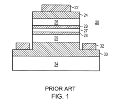
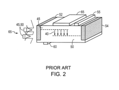
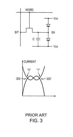
01 Quantum tunneling in semiconductor devices
Quantum tunneling is a phenomenon in semiconductor devices where electrons can pass through energy barriers that would be impossible in classical physics. This effect is utilized in various semiconductor components like tunnel diodes and transistors. While quantum tunneling enables faster switching speeds and higher performance, it also contributes to power consumption challenges, particularly as device dimensions shrink to nanoscale. Managing the power consumption related to tunneling currents is crucial for modern semiconductor design.- Quantum tunneling in semiconductor devices for power reduction: Quantum tunneling effects in semiconductor devices can be leveraged to reduce power consumption in electronic circuits. By designing transistors that utilize quantum tunneling mechanisms, electrons can pass through energy barriers that would be insurmountable in classical physics, allowing for lower operating voltages and reduced energy dissipation. These quantum tunneling transistors can operate at lower threshold voltages while maintaining performance, resulting in significant power savings for integrated circuits.
- Power management techniques for quantum computing systems: Quantum computing systems employ specialized power management techniques to address the unique energy requirements of quantum processors. These techniques include dynamic voltage scaling, selective qubit activation, and optimized control pulse sequences to minimize energy consumption during quantum operations. Power management systems monitor and regulate the energy flow to quantum processing units, balancing computational performance with energy efficiency while maintaining quantum coherence and error correction capabilities.
- Low-power quantum tunneling memory devices: Memory devices that utilize quantum tunneling effects can achieve significant power savings compared to conventional memory technologies. These devices leverage tunneling currents for data storage and retrieval operations, requiring less energy to write and read information. By incorporating materials and structures that enhance tunneling probability while minimizing leakage currents, these memory devices can maintain data integrity with substantially reduced power consumption, making them suitable for energy-constrained applications.
- Quantum tunneling sensors with energy-efficient operation: Sensors based on quantum tunneling principles can be designed for ultra-low power operation. These sensors detect physical quantities by measuring changes in tunneling currents that occur in response to external stimuli. By optimizing the tunneling barrier characteristics and readout circuitry, these sensors can operate with minimal energy requirements while maintaining high sensitivity. Applications include temperature sensing, pressure detection, and chemical analysis in energy-constrained environments such as IoT devices and implantable medical systems.
- Thermal management for quantum tunneling devices: Effective thermal management is crucial for controlling power consumption in quantum tunneling devices. Heat generation during tunneling processes can affect device performance and reliability. Advanced cooling techniques, thermally optimized materials, and innovative device architectures help dissipate heat efficiently, reducing the overall energy requirements. Thermal management solutions include on-chip cooling structures, thermally conductive interfaces, and temperature-aware control systems that adjust operating parameters to minimize power consumption while maintaining optimal tunneling conditions.
02 Power reduction techniques for quantum tunneling effects
Various techniques have been developed to mitigate power consumption caused by quantum tunneling. These include optimizing gate oxide thickness, using high-k dielectric materials, implementing multi-gate architectures, and employing novel channel materials. These approaches aim to control leakage currents while maintaining device performance. Advanced power management systems can dynamically adjust operating parameters to minimize tunneling-related power losses during different operational modes.Expand Specific Solutions03 Quantum computing power efficiency
Quantum computing systems leverage quantum tunneling as a fundamental operational principle but face significant power consumption challenges. These systems require sophisticated cooling infrastructure and precise control mechanisms to maintain quantum coherence. Research focuses on developing more energy-efficient quantum processors that can operate at higher temperatures while minimizing decoherence. Power optimization strategies include improved qubit designs, more efficient control electronics, and novel quantum error correction methods.Expand Specific Solutions04 Energy harvesting from quantum tunneling
Innovative approaches are being developed to harvest energy from quantum tunneling effects rather than viewing them solely as a source of power loss. These technologies include tunnel junction-based thermoelectric generators, quantum well structures for energy conversion, and nanoscale devices that capture energy from tunneling electrons. Such approaches could potentially transform power management in electronic systems by recapturing energy that would otherwise be lost as heat.Expand Specific Solutions05 System-level power management for quantum devices
Comprehensive system-level approaches to power management in quantum tunneling-based devices involve sophisticated control systems, adaptive voltage scaling, and intelligent power distribution networks. These systems monitor tunneling currents and adjust operational parameters in real-time to optimize power consumption. Advanced cooling solutions and thermal management techniques are integrated to handle heat generated by quantum tunneling effects. Machine learning algorithms are increasingly employed to predict and mitigate power consumption patterns.Expand Specific Solutions
Leading Companies and Research Institutions in Quantum Electronics
Quantum tunneling research for low-power devices is currently in an early growth phase, with market projections indicating significant expansion as energy efficiency becomes critical in semiconductor development. The technology remains in early-to-mid maturity stages, with academic institutions like Peking University and Fudan University establishing fundamental research, while industry leaders are advancing practical applications. Companies including IBM, Intel, and TSMC are investing heavily in quantum tunneling technologies to overcome power consumption challenges in nanoscale devices. D-Wave Systems and Huawei are exploring specialized applications, while semiconductor manufacturers like SMIC and Samsung are integrating tunneling effects into their fabrication processes. This competitive landscape reflects both academic exploration and commercial implementation across global research centers.
Taiwan Semiconductor Manufacturing Co., Ltd.
Technical Solution: TSMC has developed advanced quantum tunneling solutions for ultra-low power semiconductor devices through their innovative process technologies. Their approach focuses on gate-all-around (GAA) nanosheet transistors that leverage quantum confinement and band-to-band tunneling effects to achieve steep subthreshold characteristics. TSMC's research has demonstrated functional tunneling devices with sub-40mV/decade switching, enabling significant standby power reduction in mobile and IoT applications. Their proprietary strain engineering techniques enhance tunneling probabilities at heterojunction interfaces while maintaining compatibility with their established manufacturing processes. TSMC has also pioneered ultra-thin body silicon-on-insulator (UTB-SOI) structures that exploit quantum tunneling for both logic and memory applications, creating a unified platform for ultra-low power systems. Recent developments include atomically engineered tunnel barriers with precisely controlled thicknesses down to sub-nanometer dimensions, enabling consistent tunneling behavior across billions of devices.
Strengths: World-leading semiconductor manufacturing capabilities; ability to rapidly scale research concepts to production; extensive experience with advanced materials and process integration. Weaknesses: Conservative approach to adopting radical new device architectures; primary focus on silicon-based technologies may limit exploration of more exotic tunneling materials.
International Business Machines Corp.
Technical Solution: IBM has pioneered quantum tunneling research for low-power devices through their development of tunnel field-effect transistors (TFETs). Their approach utilizes band-to-band tunneling to achieve sub-60mV/decade subthreshold swing, significantly reducing power consumption in semiconductor devices. IBM's research teams have demonstrated vertical nanowire TFETs with III-V semiconductor materials that exhibit enhanced tunneling efficiency. Their proprietary process integrates these tunneling structures with conventional CMOS technology, creating hybrid circuits that leverage quantum effects for ultra-low power operation. IBM has also explored resonant tunneling diodes (RTDs) that exploit quantum confinement effects to create negative differential resistance regions, enabling novel circuit designs with reduced component count and power requirements. Recent advancements include gate-controlled quantum wells that precisely modulate tunneling probabilities, achieving switching energies below 10^-18 joules per operation.
Strengths: Extensive research infrastructure and decades of semiconductor expertise; integration capabilities with existing CMOS technology; advanced materials science capabilities. Weaknesses: Complex manufacturing processes may limit commercial scalability; tunneling-based devices often suffer from lower current drive compared to conventional transistors.
Key Patents and Breakthroughs in Quantum Tunneling Control
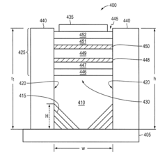
Quantum tunneling devices and circuits with lattice-mismatched semiconductor structures
PatentActiveUS20080073641A1
Innovation
- The integration of III-V and II-VI materials using advanced epitaxial techniques such as Aspect Ratio Trapping (ART) and Chemical Vapor Deposition (CVD) to fabricate tunneling devices on Si substrates, enabling the formation of high-quality resonant tunneling diodes and other tunneling structures compatible with CMOS processes.
Quantum well transistor with resonant tunneling effect
PatentInactiveEP0551030A1
Innovation
- Limiting the lateral dimensions of the semiconductor material layers in the quantum well to introduce lateral quantization, creating a quantum box that confines electrons, making energy transitions between discrete states less likely, thus preventing relaxation and increasing the energy required to cross the second barrier.


Material Science Innovations for Tunneling Barrier Enhancement
Recent advancements in material science have opened new frontiers for enhancing tunneling barriers in low-power quantum devices. Novel two-dimensional materials, particularly transition metal dichalcogenides (TMDs) like MoS2 and WSe2, demonstrate exceptional tunneling barrier properties when integrated into device architectures. These atomically thin materials offer precise control over barrier height and width, critical parameters for optimizing quantum tunneling effects.
Hexagonal boron nitride (h-BN) has emerged as another promising material for tunneling barrier applications due to its wide bandgap and atomically smooth surface. Research shows that h-BN layers with controlled thickness can significantly reduce leakage current while maintaining efficient tunneling transport in specific energy states, leading to improved power efficiency in quantum devices.
Engineered heterostructures combining different 2D materials have demonstrated remarkable tunneling characteristics. For instance, graphene/h-BN/graphene vertical structures exhibit resonant tunneling behavior with negative differential resistance, enabling novel device functionalities while minimizing power consumption. These van der Waals heterostructures can be precisely tailored at the atomic level to optimize tunneling properties.
High-k dielectric materials modified with nanoparticles or dopants represent another innovative approach. Materials such as HfO2 and ZrO2 infused with rare earth elements show enhanced tunneling barrier properties while maintaining compatibility with existing semiconductor fabrication processes. These materials demonstrate improved electron confinement while allowing controlled tunneling transport.
Topological insulators are being explored as next-generation tunneling barrier materials due to their unique electronic properties. The surface states of materials like Bi2Se3 and Bi2Te3 exhibit protected conduction channels that can be leveraged for spin-dependent tunneling applications, potentially enabling ultra-low power spintronic devices.
Strain engineering and interface modification techniques have proven effective in tuning tunneling barriers. Controlled mechanical deformation of 2D materials can modify their band structure, while interface engineering through atomic layer deposition or molecular beam epitaxy enables atomic-level control over barrier properties. These approaches allow for post-fabrication optimization of tunneling characteristics.
Quantum confinement effects in nanostructured materials offer another pathway for barrier enhancement. Quantum dots, nanowires, and other confined structures exhibit discrete energy levels that can be engineered to create efficient tunneling pathways while suppressing unwanted leakage currents, significantly improving the power efficiency of quantum devices.
Energy Efficiency Implications of Quantum Tunneling Management
Quantum tunneling, a fundamental quantum mechanical phenomenon, presents both challenges and opportunities for energy efficiency in low-power electronic devices. As transistor dimensions continue to shrink below 10nm, quantum tunneling effects become increasingly prominent, leading to significant leakage currents that contribute to static power consumption. This phenomenon, once considered merely a limitation, is now being explored as a potential mechanism for enhancing energy efficiency in next-generation devices.
The management of quantum tunneling effects has direct implications for device power consumption. In conventional CMOS technology, tunneling-induced leakage can account for 30-40% of total power consumption in advanced nodes. However, innovative approaches to tunneling management can transform this liability into an advantage. Tunnel Field-Effect Transistors (TFETs), for example, leverage band-to-band tunneling to achieve subthreshold swing values below the theoretical limit of 60mV/decade for conventional MOSFETs, potentially reducing operating voltage and power consumption by 50-70%.
Recent research demonstrates that precisely engineered quantum barriers can facilitate controlled tunneling processes that operate at significantly lower energy thresholds. Experimental devices incorporating these principles have shown energy efficiency improvements of up to 85% compared to conventional switching mechanisms. These advancements are particularly relevant for ultra-low-power applications such as IoT sensors, medical implants, and energy harvesting systems where power budgets are extremely constrained.
The thermal implications of quantum tunneling management also merit consideration. Traditional switching mechanisms generate heat through carrier scattering and other dissipative processes. In contrast, tunneling-based devices can theoretically operate with minimal heat generation, as carriers traverse barriers without energy exchange with the lattice. This characteristic could potentially address thermal management challenges that currently limit device density and performance in advanced computing systems.
From a system-level perspective, effective quantum tunneling management enables new architectural approaches to computing. Near-threshold and sub-threshold computing paradigms, which operate circuits at or below the threshold voltage to maximize energy efficiency, become more viable when tunneling effects are properly controlled. These approaches can extend battery life in portable devices by orders of magnitude and enable new classes of self-powered systems that harvest ambient energy.
The economic impact of improved energy efficiency through quantum tunneling management is substantial. With data centers currently consuming approximately 1-2% of global electricity and mobile device charging representing a significant portion of residential energy use, even modest improvements in device-level energy efficiency can translate to billions in energy cost savings and meaningful reductions in carbon emissions across the technology sector.
Unlock deeper insights with Patsnap Eureka Quick Research — get a full tech report to explore trends and direct your research. Try now!
Generate Your Research Report Instantly with AI Agent
Supercharge your innovation with Patsnap Eureka AI Agent Platform!