Roadmap For Next-Generation CSAC: Photonic Integration And Optical Clocks
AUG 29, 20259 MIN READ
Generate Your Research Report Instantly with AI Agent
Patsnap Eureka helps you evaluate technical feasibility & market potential.
CSAC Evolution and Integration Goals
Chip-Scale Atomic Clocks (CSACs) have evolved significantly since their inception in the early 2000s, transforming from laboratory curiosities to commercially available precision timing devices. The evolution trajectory has been marked by progressive miniaturization, reduced power consumption, and enhanced stability performance. First-generation CSACs focused primarily on achieving fundamental functionality within compact form factors, while second-generation devices emphasized improved performance metrics and manufacturing scalability.
The current technological landscape presents a critical inflection point for CSAC development. Traditional CSAC architectures based on coherent population trapping (CPT) in alkali vapor cells have approached theoretical performance limits within their existing design paradigms. This technological plateau necessitates fundamental innovations to achieve next-generation performance targets, particularly in stability, size reduction, and power efficiency.
Looking forward, the integration goals for next-generation CSACs center on two transformative approaches: photonic integration and optical clock technologies. Photonic integration aims to replace discrete optical components with integrated photonic circuits, potentially reducing size by an order of magnitude while simultaneously improving thermal management and mechanical stability. This approach leverages advances in silicon photonics and integrated optoelectronics to create highly compact, robust atomic clock architectures.
Optical clock technologies represent a paradigm shift from microwave to optical frequency references, offering theoretical stability improvements of 2-3 orders of magnitude. The goal is to adapt optical lattice clock principles to chip-scale implementations through novel atom trapping mechanisms and miniaturized optical frequency combs.
A critical integration objective involves developing hybrid architectures that combine traditional CSAC technologies with emerging photonic and optical approaches. This evolutionary pathway allows for incremental performance improvements while the more revolutionary technologies mature. Specific technical targets include achieving short-term stability below 1×10^-11 at one second, volume reduction to under 5 cm³, and power consumption below 50 mW.
The roadmap also emphasizes enhanced environmental resilience, particularly to vibration, temperature fluctuations, and magnetic field variations. These improvements are essential for expanding CSAC applications in dynamic environments such as autonomous vehicles, portable field equipment, and space systems.
Ultimately, the integration goals extend beyond performance metrics to address manufacturing scalability, reliability, and cost-effectiveness. The vision is to transition CSACs from specialized, high-cost devices to ubiquitous timing solutions that can be widely deployed across diverse technological domains, from telecommunications infrastructure to consumer electronics.
Market Analysis for Miniaturized Atomic Clocks
The global market for miniaturized atomic clocks has experienced significant growth in recent years, driven by increasing demand for precise timing solutions in various applications. The Chip-Scale Atomic Clock (CSAC) market, valued at approximately $400 million in 2022, is projected to reach $700 million by 2028, representing a compound annual growth rate of 9.8% during the forecast period.
Defense and aerospace sectors currently dominate the CSAC market, accounting for nearly 45% of total demand. These industries require ultra-precise timing for mission-critical operations, secure communications, and navigation systems. The telecommunications sector follows closely, constituting about 30% of the market share, where CSACs are essential for network synchronization and 5G infrastructure development.
Emerging applications in autonomous vehicles, quantum computing, and the Internet of Things (IoT) are creating new market opportunities. The autonomous vehicle market alone is expected to drive a 15% increase in CSAC demand over the next five years as these systems require nanosecond-level timing precision for safe operation and accurate positioning.
Geographically, North America leads the market with approximately 40% share, followed by Europe (25%) and Asia-Pacific (20%). However, the Asia-Pacific region is witnessing the fastest growth rate at 12.3% annually, primarily due to increasing investments in telecommunications infrastructure and defense modernization programs in countries like China, Japan, and India.
The market exhibits a concentrated competitive landscape with key players including Microsemi (now part of Microchip Technology), Frequency Electronics, Oscilloquartz, and Spectratime collectively holding over 65% market share. Recent market entry by companies like AccuBeat and Quantum SA has intensified competition, particularly in the commercial applications segment.
Price sensitivity remains a significant market constraint, with current CSAC units ranging from $1,500 to $5,000 depending on specifications. This high cost limits widespread adoption in consumer applications. Industry analysts predict that advancements in photonic integration and optical clock technologies could potentially reduce manufacturing costs by 30-40% within the next decade, expanding market accessibility.
Customer requirements are evolving toward smaller form factors, lower power consumption, and enhanced performance metrics. The next generation of CSACs incorporating photonic integration is anticipated to address these demands, potentially opening new market segments worth an estimated $300 million by 2030.
Photonic Integration Challenges in CSAC
Photonic integration in Chip-Scale Atomic Clocks (CSACs) faces significant technical challenges that must be overcome to realize the next generation of miniaturized, high-performance atomic timekeeping devices. The fundamental challenge lies in integrating optical components that traditionally occupy substantial space into a chip-scale form factor while maintaining or improving performance metrics.
Material compatibility presents a major hurdle, as the integration of III-V semiconductors (for lasers) with silicon photonics platforms requires sophisticated heterogeneous integration techniques. Current approaches include wafer bonding and epitaxial growth, but these methods often introduce thermal expansion mismatches and interface defects that degrade optical performance and long-term reliability.
Thermal management emerges as another critical challenge. The proximity of heat-generating components like lasers to temperature-sensitive elements such as vapor cells can cause frequency instabilities and drift. Conventional thermal isolation techniques become increasingly difficult to implement as device dimensions shrink below millimeter scale, necessitating novel approaches to thermal design and active temperature control within extremely confined spaces.
Packaging complexity increases exponentially with integration density. Hermetic sealing requirements for alkali vapor cells must coexist with optical coupling interfaces and electrical connections, creating competing design constraints. Current packaging solutions often compromise performance to achieve miniaturization, resulting in reduced quality factors and increased power consumption.
Optical coupling losses represent a significant efficiency barrier. The transition between different optical waveguide structures and free-space regions introduces insertion losses that can exceed 3dB per interface. These losses compound throughout the system, severely limiting overall power efficiency and signal-to-noise ratios in detection schemes.
Manufacturing scalability remains problematic for integrated CSACs. Current fabrication approaches often rely on hybrid assembly techniques that are difficult to translate to high-volume production. The precision alignment requirements between optical components (typically sub-micron) exceed standard electronic assembly tolerances by orders of magnitude.
Polarization management presents unique challenges in integrated photonic platforms. Many CSAC designs rely on precise polarization states for optimal atomic interactions, but integrated waveguides often exhibit polarization-dependent losses and birefringence that vary with temperature and mechanical stress, complicating stable operation.
The path toward overcoming these integration challenges will require interdisciplinary approaches combining advances in materials science, nanofabrication techniques, and novel optical designs specifically optimized for the atomic physics requirements of next-generation CSACs.
Current Photonic Integration Approaches for CSAC
01 Miniaturization techniques for CSAC
Various techniques are employed to reduce the size of chip-scale atomic clocks, including the use of MEMS technology, integrated photonics, and advanced packaging methods. These approaches allow for the miniaturization of key components such as vapor cells, lasers, and photodetectors while maintaining clock performance. The reduced form factor enables integration into portable devices and space-constrained applications where traditional atomic clocks would be impractical.- Miniaturization techniques for CSAC: Various techniques are employed to miniaturize chip-scale atomic clocks, including the use of MEMS technology, integrated photonics, and advanced packaging methods. These approaches allow for significant size reduction while maintaining functionality. Miniaturization efforts focus on reducing the size of key components such as the physics package, vapor cells, and control electronics, enabling the development of compact atomic clocks suitable for portable applications and space-constrained environments.
- Stability enhancement methods: Stability in chip-scale atomic clocks is achieved through various methods including temperature compensation, vibration isolation, and advanced control algorithms. These techniques help maintain frequency stability over time and under varying environmental conditions. Improved stability is critical for applications requiring precise timing over extended periods, such as telecommunications, navigation systems, and scientific instrumentation. Enhanced stability methods often involve feedback mechanisms that continuously adjust the clock's operation to compensate for external influences.
- Precision improvement innovations: Innovations to improve the precision of chip-scale atomic clocks include advanced quantum interrogation techniques, improved laser stabilization methods, and enhanced signal processing algorithms. These advancements enable CSACs to achieve higher accuracy and lower uncertainty in time measurement. Precision improvements often involve optimizing the atomic resonance detection and reducing noise sources that can degrade performance. These innovations are crucial for applications requiring extremely accurate timing, such as GPS systems and scientific research.
- Power consumption optimization: Optimizing power consumption in chip-scale atomic clocks involves developing energy-efficient components, implementing power management strategies, and creating low-power operational modes. These approaches extend battery life in portable applications while maintaining clock performance. Power optimization techniques include pulsed operation of the physics package, efficient laser driving circuits, and intelligent power scaling based on application requirements. Reduced power consumption is essential for enabling CSACs in battery-powered devices and energy-constrained systems.
- Environmental resilience enhancements: Enhancing the environmental resilience of chip-scale atomic clocks involves developing technologies that maintain performance across varying temperatures, magnetic fields, and mechanical stresses. These improvements include advanced shielding techniques, compensation algorithms, and robust packaging solutions. Environmental resilience is critical for CSACs deployed in harsh conditions such as aerospace, military applications, and industrial environments. Enhanced designs incorporate features that isolate the sensitive atomic physics from external disturbances while maintaining the compact form factor.
02 Stability enhancement methods
Improving the long-term stability of CSACs involves advanced frequency control algorithms, temperature compensation techniques, and environmental isolation strategies. These methods help maintain accurate timekeeping despite external disturbances such as vibration, temperature fluctuations, and magnetic field variations. Enhanced stability is crucial for applications requiring precise timing over extended periods, such as telecommunications infrastructure and navigation systems.Expand Specific Solutions03 Precision optimization approaches
Precision in CSACs is optimized through quantum coherence techniques, improved laser frequency stabilization, and advanced signal processing methods. These approaches reduce noise and improve the clock's short-term stability and accuracy. Higher precision enables more demanding applications in scientific instrumentation, secure communications, and high-precision timing networks where nanosecond-level accuracy is required.Expand Specific Solutions04 Power consumption reduction
Reducing power consumption in CSACs involves innovative circuit designs, low-power laser sources, and efficient thermal management techniques. These developments enable longer battery life in portable applications and reduce heat generation, which can affect clock stability. Lower power requirements make CSACs viable for deployment in energy-constrained environments such as satellites, unmanned vehicles, and remote sensing platforms.Expand Specific Solutions05 Integration with other systems
CSACs are increasingly designed for seamless integration with other electronic systems, including GNSS receivers, communication equipment, and instrumentation. This integration involves standardized interfaces, compatible form factors, and robust performance under varying operating conditions. The ability to integrate CSACs with existing systems enhances overall system performance while minimizing size, weight, and power requirements in complex applications.Expand Specific Solutions
Leading Organizations in CSAC Development
The next-generation Chip-Scale Atomic Clock (CSAC) technology landscape is currently in a transitional phase, evolving from traditional atomic clock designs toward integrated photonic solutions and optical clocks. The market is experiencing moderate growth, projected to expand significantly as miniaturization and power efficiency improve. Leading research institutions like MIT, Caltech, and University of California are driving fundamental innovations, while companies including Huawei, TSMC, and GlobalFoundries are developing the necessary semiconductor and photonic integration capabilities. Teledyne Scientific and Honeywell represent established players with expertise in precision timing, while emerging companies like Vanguard Automation and Aeponyx are pioneering specialized photonic integration solutions. The technology remains in early commercial maturity, with significant R&D investment focused on transitioning laboratory demonstrations to manufacturable products.
Massachusetts Institute of Technology
Technical Solution: MIT has pioneered significant advancements in next-generation Chip-Scale Atomic Clock (CSAC) technology through photonic integration and optical clocks. Their approach focuses on developing fully integrated photonic platforms that combine miniaturized optical components with atomic vapor cells. MIT researchers have demonstrated a photonic integrated circuit (PIC) that incorporates silicon nitride waveguides with rubidium vapor cells, achieving frequency stability in the 10^-12 range over integration times of several hours. The team has successfully implemented coherent population trapping (CPT) resonances on a chip, with specialized grating couplers and on-chip interferometers to precisely control the optical field interaction with alkali atoms. MIT's roadmap includes further miniaturization through MEMS-based vacuum packaging techniques and the integration of laser sources directly on the photonic chip to create a fully self-contained system.
Strengths: MIT's approach offers exceptional frequency stability while dramatically reducing size, weight, and power requirements compared to traditional atomic clocks. Their silicon photonics platform leverages existing semiconductor manufacturing infrastructure, enabling potential mass production. Weaknesses: The complete integration of all components, particularly stable laser sources, remains challenging, and the technology still faces thermal management issues that can affect long-term stability in variable environments.
Teledyne Scientific & Imaging LLC
Technical Solution: Teledyne Scientific & Imaging has developed an advanced photonically integrated CSAC platform that combines MEMS technology with specialized optical components. Their approach utilizes a proprietary silicon photonics platform that integrates multiple optical functions including beam splitting, polarization control, and photodetection on a single chip. Teledyne's solution incorporates a vertically integrated alkali vapor cell directly bonded to the photonic circuit, enabling efficient light-atom interaction while maintaining a compact form factor. The company has demonstrated clock stability reaching 10^-11 at one second integration time with drift rates below 10^-10 per day. Their roadmap includes transitioning from rubidium to strontium-based optical lattice clock technology, which promises to improve stability by several orders of magnitude. Teledyne is also developing specialized III-V integration techniques to incorporate semiconductor lasers directly onto their silicon photonic platform, eliminating the need for external optical sources and further reducing system size.
Strengths: Teledyne's solution offers exceptional ruggedness suitable for defense and aerospace applications, with demonstrated performance in high-vibration environments. Their vertical integration capabilities allow for controlled manufacturing from chip design through packaging. Weaknesses: The current technology still requires relatively high power consumption compared to purely electronic solutions, and the transition to strontium-based optical clocks introduces significant technical challenges in maintaining the required vacuum levels and optical stability in a miniaturized package.
Key Innovations in Optical Clock Technology
Optical ensembling such as for atomic clocks
PatentPendingUS20250125943A1
Innovation
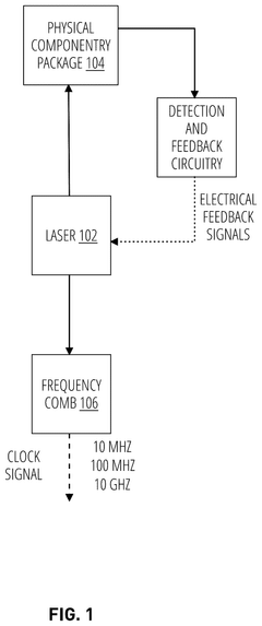
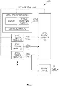
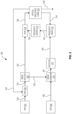
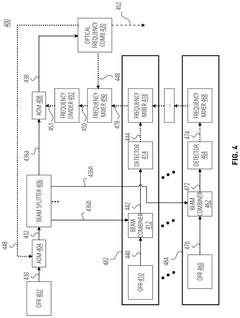
- The solution involves ensembling multiple optical atomic clocks in the optical domain to stabilize a clock signal, reducing the need for multiple expensive frequency combs and enhancing frequency stability.
Molecular clock
PatentActiveUS20190235445A1
Innovation
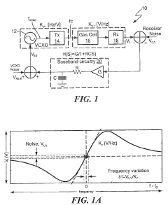
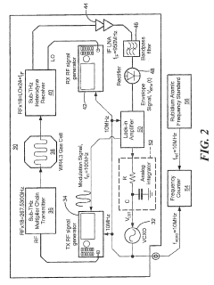
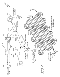
- A molecular clock utilizing rotational-state transitions of gaseous polar molecules in the sub-THz region, integrated with CMOS technology, providing a compact, low-power, and robust frequency reference with enhanced stability and instant start-up capabilities.
Quantum Technology Implications for CSAC
Quantum technologies are fundamentally reshaping the landscape of precision timing and measurement, with significant implications for Chip-Scale Atomic Clock (CSAC) development. The quantum mechanical principles that underpin atomic clocks are being enhanced through quantum information science, quantum sensing, and quantum metrology. These advancements offer pathways to overcome current CSAC limitations in stability, size, and power consumption.
Quantum entanglement and superposition principles are being leveraged to create next-generation quantum sensors that could dramatically improve CSAC performance. Specifically, quantum-enhanced measurement techniques like spin squeezing and quantum non-demolition measurements can potentially surpass the standard quantum limit, enabling unprecedented precision in frequency standards without increasing interrogation time or atom number.
The integration of quantum technologies with photonic platforms presents a particularly promising direction. Quantum photonic integrated circuits (QPICs) could enable the miniaturization of quantum optical components necessary for advanced CSAC designs. These include single-photon sources, quantum memories, and entangled photon pair generators that could be incorporated into future CSAC architectures.
Quantum networks represent another frontier with implications for CSAC technology. Distributed quantum sensing across networked CSACs could enable enhanced synchronization capabilities and improved resilience against environmental perturbations. This approach could be particularly valuable for applications requiring synchronized timing across multiple platforms or locations.
Cold atom technologies, which form the basis for optical lattice clocks and quantum gas microscopes, are being adapted for chip-scale implementations. These developments could lead to hybrid quantum-classical architectures where quantum components enhance traditional CSAC designs. The challenge lies in maintaining quantum coherence in miniaturized environments while managing power and thermal constraints.
Quantum materials research is yielding new substrates and interfaces that could improve the performance of key CSAC components. Materials exhibiting quantum properties such as topological protection or enhanced coherence times could lead to more robust clock operations in challenging environments, addressing current limitations in stability under varying conditions.
The convergence of quantum technology with CSAC development is not without challenges. Quantum systems typically require extreme environmental conditions—ultra-high vacuum, cryogenic temperatures, or sophisticated laser cooling—that are difficult to achieve in compact, low-power devices. The roadmap for quantum-enhanced CSACs must therefore include innovations in quantum engineering that address these practical constraints while leveraging quantum advantages.
Space and Defense Applications of Next-Gen CSAC
The integration of next-generation Chip-Scale Atomic Clocks (CSACs) into space and defense systems represents a transformative advancement in precision timing capabilities for critical applications. These miniaturized atomic clocks, enhanced through photonic integration and optical clock technologies, offer unprecedented performance characteristics that address the unique challenges of space and defense environments.
In space applications, next-generation CSACs provide essential timing solutions for satellite navigation systems, enabling more precise positioning capabilities. The reduced size, weight, and power (SWaP) requirements of these advanced CSACs make them particularly valuable for small satellite constellations and CubeSats, where resource constraints are significant. The improved long-term stability of optical-based CSACs also reduces the need for frequent synchronization with ground stations, enhancing autonomous operation capabilities of spacecraft during extended missions.
For deep space exploration, the enhanced performance of next-generation CSACs supports more accurate ranging and navigation, critical for missions to distant planets and interplanetary trajectories. The improved resistance to radiation effects through photonic integration techniques ensures reliable operation in the harsh radiation environment of space, extending operational lifetimes and reducing mission risks.
In defense applications, these advanced timing solutions enable enhanced military communications systems that require precise synchronization for frequency-hopping spread spectrum techniques and secure communications protocols. The improved jamming resistance of systems utilizing next-generation CSACs provides critical advantages in contested electromagnetic environments, where timing disruption is an increasingly common electronic warfare tactic.
For guided munitions and unmanned systems, the miniaturized form factor allows integration into smaller platforms while maintaining navigation accuracy during GPS-denied operations. This capability is increasingly important as adversaries develop sophisticated GPS jamming and spoofing technologies to counter precision-guided systems.
Radar systems benefit significantly from the phase stability improvements offered by next-generation CSACs, enabling enhanced target discrimination and identification capabilities. The reduced phase noise characteristics support more sophisticated signal processing algorithms for detecting low-observable targets in cluttered environments.
The deployment of these advanced timing solutions also supports the development of distributed sensor networks for surveillance and reconnaissance, where synchronized measurements across multiple platforms enable improved situational awareness and target localization through multilateration techniques.
As military systems increasingly rely on networked operations, the precise timing provided by next-generation CSACs ensures effective coordination between platforms and systems, supporting the Joint All-Domain Command and Control (JADC2) initiatives that require seamless information sharing across previously isolated domains of warfare.
Unlock deeper insights with Patsnap Eureka Quick Research — get a full tech report to explore trends and direct your research. Try now!
Generate Your Research Report Instantly with AI Agent
Supercharge your innovation with Patsnap Eureka AI Agent Platform!
