Semiconductors in Neuromorphic Computing: Performance Analysis
OCT 27, 202510 MIN READ
Generate Your Research Report Instantly with AI Agent
PatSnap Eureka helps you evaluate technical feasibility & market potential.
Neuromorphic Computing Semiconductor Evolution and Objectives
Neuromorphic computing represents a paradigm shift in computational architecture, drawing inspiration from the human brain's neural networks to create more efficient and powerful computing systems. The evolution of semiconductors specifically designed for neuromorphic applications has been marked by significant milestones over the past several decades, transitioning from traditional von Neumann architectures toward more brain-inspired designs.
The journey began in the late 1980s with Carver Mead's pioneering work on neuromorphic engineering, which established the foundational concepts for hardware implementations of neural systems. Early implementations relied on conventional CMOS technology, adapted to mimic neural behaviors through specialized circuit designs. These initial efforts demonstrated the potential of brain-inspired computing but were limited by the constraints of existing semiconductor technologies.
The 2000s witnessed the emergence of dedicated neuromorphic chips, such as IBM's TrueNorth and Intel's Loihi, which represented significant advances in specialized hardware for neural computation. These developments coincided with breakthroughs in materials science and semiconductor fabrication techniques that enabled more efficient implementation of synaptic functions in hardware.
Recent years have seen an acceleration in neuromorphic semiconductor development, driven by the convergence of several technological trends: the slowing of Moore's Law, increasing demand for edge computing capabilities, and advances in artificial intelligence algorithms. This has led to exploration of novel materials and device physics beyond traditional silicon, including memristors, phase-change materials, and spintronic devices, which can more naturally emulate the behavior of biological neurons and synapses.
The primary objective of neuromorphic semiconductor development is to create computing systems that combine the adaptability and energy efficiency of biological neural networks with the speed and reliability of electronic systems. Specific goals include reducing power consumption by several orders of magnitude compared to conventional computing architectures, enabling on-chip learning and adaptation, and supporting massively parallel processing of sensory data.
Current research focuses on addressing several key challenges: scaling neuromorphic systems to incorporate billions of artificial neurons and synapses, improving the fidelity of neural and synaptic models in hardware, developing more efficient training algorithms for neuromorphic hardware, and creating standardized benchmarks for performance evaluation.
The trajectory of neuromorphic semiconductor evolution points toward increasingly specialized hardware that can support a wide range of applications, from autonomous systems and robotics to advanced pattern recognition and natural language processing, while maintaining exceptional energy efficiency and real-time processing capabilities.
Market Analysis for Brain-Inspired Computing Solutions
The neuromorphic computing market is experiencing significant growth, driven by increasing demand for AI applications that require efficient processing of complex neural networks. Current market valuations place the global neuromorphic computing sector at approximately 3.2 billion USD in 2023, with projections indicating a compound annual growth rate of 23.7% through 2030. This growth trajectory is supported by substantial investments from both private and public sectors, with government initiatives in the US, EU, and China allocating dedicated funding for brain-inspired computing research and development.
Market segmentation reveals diverse application domains for neuromorphic semiconductor solutions. The healthcare sector represents the largest market share at 28%, where neuromorphic systems are being deployed for medical imaging analysis, patient monitoring, and drug discovery. Autonomous vehicles follow closely at 24%, utilizing these systems for real-time decision making and sensor fusion. Industrial automation and robotics account for 19%, while security and surveillance applications comprise 15% of the market. Emerging applications in consumer electronics and IoT devices represent the fastest-growing segment with a 34% year-over-year increase.
Customer demand analysis indicates a shift in priorities from traditional computing metrics to neuromorphic-specific performance indicators. End-users increasingly value energy efficiency (measured in operations per watt) over raw processing speed, with 67% of enterprise customers citing power consumption as their primary concern. Latency requirements vary significantly across applications, with edge computing implementations demanding response times under 10 milliseconds, while cloud-based applications can tolerate higher latencies.
Regional market analysis shows North America leading with 42% market share, followed by Europe (27%), Asia-Pacific (24%), and rest of the world (7%). However, the Asia-Pacific region demonstrates the highest growth rate at 29.3% annually, driven by aggressive semiconductor manufacturing investments in Taiwan, South Korea, and China. Japan's neuromorphic computing market is particularly focused on robotics applications, while India is emerging as a significant consumer for AI-enabled healthcare solutions.
Competitive landscape assessment reveals a market dominated by established semiconductor manufacturers who have pivoted toward neuromorphic designs, alongside specialized startups focused exclusively on brain-inspired architectures. The five largest players control approximately 63% of market share, though this concentration is expected to decrease as new entrants introduce innovative solutions. Market barriers include high initial development costs, intellectual property challenges, and the need for specialized expertise in both neuroscience and semiconductor design.
Current Semiconductor Technologies and Limitations in Neuromorphic Systems
Current semiconductor technologies in neuromorphic computing primarily rely on CMOS (Complementary Metal-Oxide-Semiconductor) platforms, which have been optimized for conventional von Neumann computing architectures. While these technologies have enabled initial neuromorphic implementations, they face significant limitations when attempting to emulate the brain's efficiency and functionality. Traditional CMOS-based neuromorphic systems consume orders of magnitude more power than biological neural systems, with energy requirements typically in the picojoule range per synaptic operation compared to femtojoules in biological systems.
Memory-processor bottlenecks represent another critical limitation in current semiconductor implementations. The physical separation between memory and processing units creates significant data transfer overhead, fundamentally limiting the parallelism and energy efficiency that neuromorphic systems aim to achieve. This bottleneck becomes particularly problematic when implementing large-scale neural networks with millions or billions of parameters.
Emerging non-volatile memory technologies such as Resistive RAM (RRAM), Phase Change Memory (PCM), and Magnetic RAM (MRAM) offer promising alternatives for neuromorphic implementations. These technologies enable in-memory computing paradigms that can potentially overcome the von Neumann bottleneck. However, they currently face challenges related to device variability, limited endurance, and integration complexity with standard CMOS processes.
Silicon photonics represents another promising direction, offering ultra-high bandwidth and inherent parallelism for neuromorphic computing. Photonic neuromorphic chips can potentially perform matrix operations at the speed of light with minimal energy consumption. However, current photonic implementations struggle with miniaturization, thermal management, and integration with electronic control systems.
Specialized neuromorphic hardware like IBM's TrueNorth, Intel's Loihi, and BrainChip's Akida demonstrate the potential of dedicated neuromorphic architectures. These chips implement spiking neural networks (SNNs) directly in hardware, achieving significant improvements in energy efficiency. Nevertheless, they still face challenges in scaling, programming complexity, and application-specific optimization.
3D integration and advanced packaging technologies are being explored to overcome some of these limitations by enabling denser interconnections between computing elements. However, thermal management becomes increasingly challenging as integration density increases, potentially limiting the practical scalability of such approaches.
The fundamental challenge remains bridging the gap between the deterministic, binary nature of conventional semiconductors and the stochastic, analog nature of biological neural systems. Current technologies struggle to efficiently implement the massive parallelism, sparse activity patterns, and adaptive learning mechanisms that make biological brains so efficient for cognitive tasks.
Existing Semiconductor Solutions for Neural Network Implementation
01 Semiconductor material composition and processing
The composition and processing of semiconductor materials significantly impact their performance. Various techniques are employed to enhance semiconductor properties, including doping, alloying, and thermal treatments. These processes can modify the electrical conductivity, band gap, and carrier mobility of semiconductors, resulting in improved device performance. Advanced material processing methods enable the creation of high-quality semiconductor structures with fewer defects and better crystallinity.- Semiconductor material composition and processing: Various compositions and processing methods can enhance semiconductor performance. This includes specialized material formulations, doping techniques, and thermal treatments that modify the electrical properties of semiconductors. Advanced processing techniques can reduce defects, improve crystallinity, and optimize carrier mobility, resulting in better overall semiconductor performance.
- Semiconductor device structures and packaging: The physical structure and packaging of semiconductor devices significantly impact their performance. Innovations in device architecture, contact design, and packaging techniques can improve thermal management, reduce parasitic effects, and enhance electrical characteristics. Advanced packaging solutions protect the semiconductor while facilitating efficient heat dissipation and electrical connectivity.
- Semiconductor manufacturing techniques: Manufacturing processes directly influence semiconductor performance. Precision fabrication methods, including lithography, etching, deposition, and planarization techniques, affect device characteristics. Innovations in manufacturing equipment and methodologies can reduce variability, increase yield, and enhance the performance of semiconductor devices.
- Semiconductor performance enhancement through electronic design: Electronic design approaches can optimize semiconductor performance. This includes circuit design techniques, power management strategies, and signal integrity considerations that maximize the capabilities of semiconductor devices. Advanced design methodologies account for semiconductor physics to achieve higher speeds, lower power consumption, and improved reliability.
- Novel semiconductor materials and structures: Emerging semiconductor materials and novel structures offer pathways to enhanced performance. These include compound semiconductors, two-dimensional materials, quantum structures, and engineered bandgap materials. Such innovations can overcome the limitations of traditional silicon-based semiconductors, enabling higher speeds, better energy efficiency, and operation in extreme environments.
02 Semiconductor device structures and fabrication
Innovative semiconductor device structures and fabrication techniques contribute to enhanced performance. These include advanced transistor architectures, novel interconnect designs, and specialized packaging methods. Miniaturization and 3D integration allow for higher component density and improved signal transmission. Precision manufacturing processes such as lithography, etching, and deposition are crucial for creating high-performance semiconductor devices with optimized electrical characteristics.Expand Specific Solutions03 Thermal management in semiconductors
Effective thermal management is essential for maintaining semiconductor performance. Heat dissipation techniques include specialized packaging materials, thermal interface materials, and cooling systems. Managing temperature during operation prevents performance degradation and extends device lifespan. Advanced thermal solutions enable semiconductors to operate at higher power densities without compromising reliability or efficiency.Expand Specific Solutions04 Semiconductor testing and quality control
Comprehensive testing and quality control methods ensure semiconductor performance meets specifications. These include electrical parameter testing, reliability assessment, and defect analysis. Advanced inspection techniques identify potential failure modes before device deployment. Automated testing systems enable high-throughput evaluation of semiconductor performance characteristics across various operating conditions.Expand Specific Solutions05 Next-generation semiconductor technologies
Emerging semiconductor technologies offer significant performance improvements over conventional approaches. These include wide-bandgap materials, quantum computing elements, and neuromorphic architectures. Novel semiconductor designs incorporate features that enhance energy efficiency, processing speed, and functionality. Research in areas such as spintronics, photonics integration, and two-dimensional materials is driving the development of semiconductors with unprecedented performance capabilities.Expand Specific Solutions
Leading Companies and Research Institutions in Neuromorphic Semiconductors
Neuromorphic computing is currently in an early growth phase, with the market expected to expand significantly due to increasing demand for AI applications requiring energy-efficient processing. The global market size is projected to reach approximately $8-10 billion by 2028, growing at a CAGR of over 20%. Technologically, the field remains in development with varying maturity levels across implementations. Leading players include IBM with its TrueNorth architecture, Samsung Electronics advancing memory-centric computing, Syntiant focusing on edge AI solutions, and SK hynix developing specialized memory technologies. Academic institutions like Tsinghua University, KAIST, and Caltech are driving fundamental research, while companies such as Semiconductor Energy Laboratory and Northrop Grumman are exploring specialized applications. The ecosystem reflects a blend of established semiconductor giants and specialized startups working to overcome current limitations in power efficiency and computational architecture.
Samsung Electronics Co., Ltd.
Technical Solution: Samsung has developed advanced neuromorphic computing solutions leveraging its expertise in memory technologies. Their approach centers on resistive RAM (RRAM) and magnetoresistive RAM (MRAM) technologies to create brain-inspired computing architectures. Samsung's neuromorphic chips utilize crossbar arrays of non-volatile memory cells that function as artificial synapses, enabling massively parallel analog computation. Their research demonstrates that these memory-centric neuromorphic designs can achieve energy efficiencies of less than 10 femtojoules per synaptic operation, representing orders of magnitude improvement over conventional digital approaches. Samsung has also pioneered 3D stacking techniques for neuromorphic chips, vertically integrating memory layers with processing elements to maximize density and minimize signal propagation distances. Their neuromorphic architecture incorporates spike-timing-dependent plasticity (STDP) learning mechanisms implemented directly in hardware, enabling on-chip learning capabilities that adapt to input patterns over time.
Strengths: Leverages Samsung's world-leading memory manufacturing capabilities, achieves extremely high energy efficiency through analog computing, and enables high-density integration through advanced packaging technologies. Weaknesses: Analog implementations face challenges with device variability and long-term reliability, and standardization of programming models remains a work in progress.
Syntiant Corp.
Technical Solution: Syntiant has developed the Neural Decision Processor (NDP), a specialized neuromorphic semiconductor architecture optimized for edge AI applications with extreme power efficiency. Their NDP100 and NDP200 series chips are designed specifically for always-on applications in battery-powered devices, consuming less than 1mW while performing deep learning inference. Syntiant's architecture employs a unique memory-centric design where computation occurs directly within non-volatile memory arrays, eliminating the energy-intensive data movement that plagues traditional von Neumann architectures. The company's chips achieve 100x better energy efficiency compared to conventional MCUs and DSPs for neural network processing. Their technology incorporates weight-stationary dataflow, in-memory computing, and sparse activation techniques to maximize computational efficiency while minimizing power consumption. Syntiant's solutions have been deployed in over 20 million devices worldwide.
Strengths: Ultra-low power consumption enabling always-on AI in battery-powered devices, production-proven technology with commercial deployment, and specialized optimization for audio and vision applications. Weaknesses: Limited to specific application domains (primarily keyword spotting and vision tasks) and less flexible than general-purpose neuromorphic architectures.
Critical Patents and Breakthroughs in Neuromorphic Chip Design
Semiconductor device including ferroelectric material, neuromorphic circuit including the semiconductor device, and neuromorphic computing apparatus including the neuromorphic circuit
PatentActiveUS11887989B2
Innovation
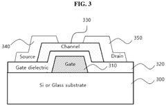
- The development of semiconductor devices and neuromorphic circuits incorporating ferroelectric materials, which enable efficient data processing by simulating synaptic functions, allowing for parallel processing and improved data storage and retrieval, thereby enhancing the accuracy and speed of data processing.
Neuromorphic semiconductor device and operating method thereof
PatentPendingUS20250157556A1
Innovation
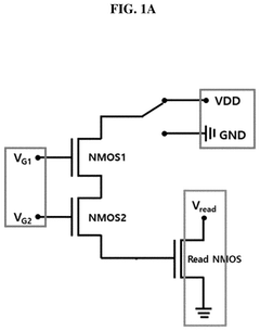
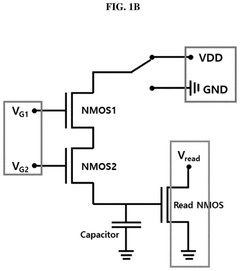
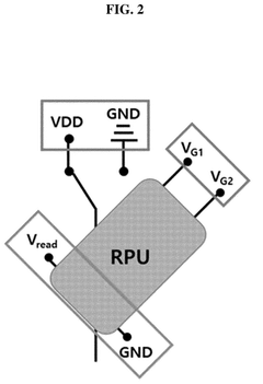
- A neuromorphic semiconductor device utilizing a resistive processing unit (RPU) with N-type metal oxide semiconductor (NMOS) elements, enabling symmetrical charging/discharging and memory updates, and reducing off-current by connecting NMOSs in series.
Energy Efficiency Benchmarks and Performance Metrics
Energy efficiency has emerged as a critical benchmark in evaluating neuromorphic computing systems, particularly those based on semiconductor technologies. Traditional von Neumann architectures consume significant power during data transfer between memory and processing units, creating a bottleneck that neuromorphic systems aim to overcome. Current benchmarks indicate that neuromorphic chips can achieve energy efficiencies of 10-100 picojoules per synaptic operation, representing orders of magnitude improvement over conventional computing platforms for neural network tasks.
Performance metrics for neuromorphic semiconductors must be evaluated across multiple dimensions. Synaptic operations per second per watt (SOPS/W) has become a standard industry metric, with leading neuromorphic chips demonstrating 10^12 to 10^14 SOPS/W. This metric directly correlates with the system's ability to perform brain-like computations efficiently. Latency measurements, typically in microseconds to milliseconds, reflect the real-time processing capabilities essential for applications like autonomous vehicles and robotics.
Area efficiency, measured in synaptic operations per square millimeter, provides insight into the scalability of neuromorphic designs. Current semiconductor implementations achieve 10^3 to 10^5 synapses per mm², though this remains orders of magnitude below biological neural density. The trade-off between density and energy efficiency represents a key optimization challenge in semiconductor design for neuromorphic systems.
Temperature stability presents another critical performance metric, as neuromorphic circuits must maintain consistent behavior across operating conditions. Silicon-based implementations typically operate reliably between -40°C and 125°C, while emerging materials like phase-change memory show promising performance but with narrower temperature ranges, impacting their deployment flexibility.
Standardized benchmarking suites have emerged to facilitate comparative analysis, including the Neuromorphic Design Benchmark (NDB) and SNN-specific performance tests. These frameworks evaluate systems on tasks ranging from simple pattern recognition to complex temporal processing, providing a holistic view of performance across different application domains.
The energy-delay product (EDP) has proven particularly valuable as a composite metric, capturing both the energy efficiency and computational speed of neuromorphic systems. Leading semiconductor implementations achieve EDPs 100-1000× better than GPU implementations for specific neural network workloads, highlighting the fundamental advantage of neuromorphic architectures for certain computational paradigms.
Integration Challenges with Conventional Computing Systems
The integration of neuromorphic computing systems based on specialized semiconductor technologies with conventional computing architectures presents significant technical challenges that must be addressed for widespread adoption. Current von Neumann architectures fundamentally differ from brain-inspired neuromorphic systems in both data processing paradigms and physical implementation. This architectural mismatch creates bottlenecks when attempting to establish seamless communication channels between these disparate computing approaches.
Interface compatibility represents a primary obstacle, as neuromorphic systems typically operate with spike-based information processing while conventional systems utilize binary logic. The translation between these fundamentally different data representations requires specialized interface circuits that can efficiently convert signals while preserving information integrity. These conversion processes inevitably introduce latency and energy overhead, potentially undermining the inherent efficiency advantages of neuromorphic systems.
Power management discrepancies further complicate integration efforts. Neuromorphic semiconductors often operate at significantly lower power levels with event-driven processing, while conventional systems maintain continuous clock-driven operations at higher voltages. Creating unified power delivery networks that can accommodate these divergent requirements demands sophisticated power management solutions that can dynamically adjust to varying computational loads across the hybrid system.
Timing synchronization presents another substantial challenge. Neuromorphic systems typically operate asynchronously with event-based processing, while conventional computing relies on precise clock synchronization. Developing reliable timing protocols that bridge these different temporal paradigms requires innovative synchronization mechanisms that can maintain system coherence without sacrificing the performance benefits of either computing approach.
Software ecosystem limitations also impede seamless integration. The programming models, development tools, and optimization techniques for neuromorphic systems remain relatively immature compared to conventional computing environments. This software gap necessitates the development of unified programming frameworks that can effectively target heterogeneous computing resources while abstracting hardware complexities from application developers.
Manufacturing integration poses additional challenges, as neuromorphic semiconductor technologies often require specialized fabrication processes that differ from standard CMOS manufacturing. Achieving cost-effective production of integrated systems may require novel packaging approaches or 3D integration technologies that can combine disparate semiconductor technologies while maintaining thermal stability and signal integrity across the system.
Addressing these integration challenges requires collaborative efforts across hardware architecture, circuit design, system software, and semiconductor manufacturing disciplines. Recent research demonstrates promising approaches through chiplet-based integration, standardized neural network interfaces, and heterogeneous computing frameworks that could eventually enable seamless cooperation between neuromorphic and conventional computing paradigms.
Unlock deeper insights with PatSnap Eureka Quick Research — get a full tech report to explore trends and direct your research. Try now!
Generate Your Research Report Instantly with AI Agent
Supercharge your innovation with PatSnap Eureka AI Agent Platform!