

Why Semiconductor Materials Dominate Neuromorphic Computing
OCT 27, 202510 MIN READ
Generate Your Research Report Instantly with AI Agent
PatSnap Eureka helps you evaluate technical feasibility & market potential.
Neuromorphic Computing Evolution and Objectives
Neuromorphic computing represents a revolutionary approach to computational architecture that draws inspiration from the structure and function of the human brain. Since its conceptual inception in the late 1980s by Carver Mead, this field has evolved significantly, transitioning from theoretical frameworks to practical implementations. The fundamental objective of neuromorphic computing is to create hardware systems that can process information in a manner analogous to biological neural networks, offering advantages in energy efficiency, parallel processing, and adaptive learning capabilities.
The evolution of neuromorphic computing can be traced through several distinct phases. Initially, research focused on understanding the basic principles of neural computation and developing simplified electronic models of neurons and synapses. This period was characterized by significant theoretical advancements but limited practical applications due to technological constraints. The second phase, beginning in the early 2000s, saw increased integration with semiconductor technologies, enabling the development of more sophisticated neuromorphic chips and systems.
In recent years, the field has experienced accelerated growth driven by advancements in semiconductor materials and fabrication techniques. Silicon-based neuromorphic chips, such as IBM's TrueNorth and Intel's Loihi, have demonstrated remarkable capabilities in pattern recognition and real-time data processing while consuming significantly less power than conventional computing systems. These developments have established semiconductors as the dominant material platform for neuromorphic computing implementations.
The primary objectives of contemporary neuromorphic computing research include achieving greater energy efficiency, enhancing computational density, improving learning capabilities, and developing more biologically accurate neural models. Energy efficiency remains particularly crucial, as the human brain operates on approximately 20 watts of power while performing complex cognitive tasks that would require megawatts of power in traditional computing systems. This efficiency gap represents both a challenge and an opportunity for semiconductor-based neuromorphic systems.
Another key objective is scalability – developing architectures that can incorporate billions of artificial neurons and trillions of synapses while maintaining efficient operation. This goal necessitates innovations in semiconductor materials and device physics to overcome the limitations of conventional CMOS technology. Additionally, researchers aim to implement more sophisticated learning algorithms directly in hardware, enabling systems that can adapt to new information without explicit programming.
The trajectory of neuromorphic computing points toward increasingly integrated systems that combine digital and analog processing elements, specialized memory structures, and novel semiconductor materials to achieve brain-like functionality. As this field continues to mature, it promises to enable new applications in artificial intelligence, robotics, and data processing that were previously impractical due to power or computational constraints.
Market Analysis for Brain-Inspired Computing Solutions
The neuromorphic computing market is experiencing significant growth, driven by increasing demand for AI applications that require efficient processing of complex neural networks. Current market projections indicate the global neuromorphic computing market will reach approximately $8.9 billion by 2025, with a compound annual growth rate of 49.1% from 2020. This remarkable growth trajectory is fueled by expanding applications in edge computing, autonomous systems, and real-time data processing scenarios where traditional computing architectures face efficiency limitations.
Semiconductor-based neuromorphic solutions currently dominate the market landscape, accounting for over 85% of commercial implementations. This dominance stems from the established semiconductor manufacturing ecosystem, which offers scalable production capabilities and integration advantages with existing computing infrastructure. Silicon-based neuromorphic chips from industry leaders like Intel, IBM, and BrainChip have demonstrated superior performance-to-power ratios compared to conventional computing architectures for specific neural network workloads.
Market segmentation reveals distinct application sectors driving adoption. The automotive industry represents the fastest-growing segment with 57% annual growth, primarily implementing neuromorphic systems for advanced driver assistance systems and autonomous vehicle perception. Healthcare applications follow at 43% growth, with neuromorphic computing enabling real-time processing of complex biosignals and medical imaging. Industrial automation and smart infrastructure sectors collectively account for approximately 31% of current market demand.
Regional analysis shows North America leading with 42% market share, followed by Europe (28%) and Asia-Pacific (24%). However, the Asia-Pacific region demonstrates the highest growth rate at 53% annually, driven by substantial investments in semiconductor manufacturing infrastructure and AI research initiatives in China, South Korea, and Japan.
Customer demand patterns indicate a clear preference for semiconductor-based solutions due to their compatibility with existing systems, established development tools, and proven reliability metrics. Enterprise surveys reveal that 76% of potential adopters prioritize integration capabilities with current infrastructure over absolute performance gains, explaining the continued market preference for semiconductor implementations despite theoretical advantages of alternative materials.
Market barriers include high initial development costs, limited standardization across platforms, and the need for specialized programming expertise. These factors have created a market environment where established semiconductor manufacturers with robust ecosystems maintain significant competitive advantages over newer entrants proposing alternative material approaches.
Semiconductor Materials in Neuromorphic Computing: Status and Challenges
Semiconductor materials have established themselves as the foundation of neuromorphic computing systems due to their unique physical properties and compatibility with existing manufacturing infrastructure. Currently, silicon-based complementary metal-oxide-semiconductor (CMOS) technology dominates the field, with companies like Intel, IBM, and BrainChip developing neuromorphic chips using advanced semiconductor processes. These materials enable the creation of artificial synapses and neurons that can mimic the brain's information processing capabilities while maintaining energy efficiency.
Despite significant progress, several technical challenges persist in semiconductor-based neuromorphic computing. The von Neumann bottleneck remains a fundamental limitation, as the separation between memory and processing units creates data transfer inefficiencies. Current semiconductor technologies struggle to fully replicate the brain's parallel processing capabilities and energy efficiency, with neuromorphic chips still consuming orders of magnitude more power per operation than biological neurons.
Scaling issues present another significant challenge. As devices shrink to nanometer scales, quantum effects and variability become increasingly problematic, affecting the reliability and predictability of neuromorphic circuits. Additionally, the integration of different semiconductor materials with varying properties introduces interface complications that can degrade performance and increase manufacturing complexity.
Material stability and endurance represent critical concerns for practical applications. Many emerging semiconductor materials for neuromorphic computing exhibit degradation over time, particularly under the repeated switching operations required for learning algorithms. This limits their long-term reliability and necessitates the development of more robust materials or compensation techniques.
Geographically, neuromorphic semiconductor research is concentrated in several key regions. The United States leads with significant investments from both government agencies like DARPA and major technology companies. Europe has established strong research clusters, particularly in Germany and Switzerland, while Asia has seen rapid growth in neuromorphic semiconductor development, with Japan, South Korea, and China making substantial investments in both research and manufacturing capabilities.
Emerging semiconductor materials such as metal oxides, chalcogenides, and two-dimensional materials are being explored as alternatives to traditional silicon. These materials offer unique properties like memristive behavior, which allows for more efficient implementation of synaptic functions. However, their integration with conventional CMOS technology presents significant manufacturing challenges that must be overcome before widespread adoption becomes feasible.
The development of heterogeneous integration techniques represents a promising approach to addressing current limitations, combining different semiconductor materials to leverage their respective advantages while mitigating individual weaknesses. This approach may provide a pathway to neuromorphic systems that more closely approximate the efficiency and functionality of biological neural networks.
Current Semiconductor-Based Neuromorphic Architectures
01 Silicon-based semiconductor materials
Silicon is one of the most widely used semiconductor materials due to its abundance, stability, and suitable electronic properties. Silicon-based semiconductors form the foundation of modern electronics, including integrated circuits, microprocessors, and various electronic devices. These materials can be doped with specific elements to modify their electrical conductivity and create p-type or n-type semiconductors essential for electronic components.- Silicon-based semiconductor materials: Silicon is one of the most widely used semiconductor materials due to its abundance, stability, and suitable electronic properties. Silicon-based semiconductors form the foundation of modern electronics, including integrated circuits, microprocessors, and various electronic devices. These materials can be doped with specific elements to modify their electrical conductivity and create p-type or n-type semiconductors essential for electronic component manufacturing.
- Compound semiconductor materials: Compound semiconductors are formed by combining elements from different groups of the periodic table, such as gallium arsenide (GaAs), gallium nitride (GaN), and indium phosphide (InP). These materials often exhibit superior electronic properties compared to silicon, including higher electron mobility and direct bandgaps, making them ideal for high-frequency applications, optoelectronics, and photovoltaics. Compound semiconductors enable the development of advanced devices like high-efficiency LEDs, laser diodes, and high-speed transistors.
- Semiconductor material processing techniques: Various processing techniques are employed to manufacture and modify semiconductor materials for specific applications. These include crystal growth methods like Czochralski process, epitaxial growth, and chemical vapor deposition (CVD). Additional processing techniques involve doping, etching, lithography, and thermal treatments to create desired semiconductor structures and properties. Advanced processing methods enable the production of high-purity semiconductor materials with precisely controlled characteristics.
- Semiconductor nanomaterials and thin films: Semiconductor nanomaterials and thin films represent an important category of semiconductor materials with unique properties due to their reduced dimensions. These include quantum dots, nanowires, nanotubes, and ultrathin semiconductor layers. The nanoscale dimensions of these materials lead to quantum confinement effects, resulting in tunable electronic and optical properties. Semiconductor nanomaterials find applications in next-generation electronics, sensors, photovoltaics, and quantum computing devices.
- Novel and emerging semiconductor materials: Research in semiconductor materials continues to evolve with the development of novel materials that offer improved performance or new functionalities. These include wide bandgap semiconductors like silicon carbide (SiC) and diamond, two-dimensional materials such as graphene and transition metal dichalcogenides, and organic semiconductors. These emerging materials enable new applications in power electronics, flexible electronics, wearable devices, and sustainable technologies, addressing limitations of traditional semiconductor materials.
02 Compound semiconductor materials
Compound semiconductors are formed by combining elements from different groups of the periodic table, such as gallium arsenide (GaAs), gallium nitride (GaN), and indium phosphide (InP). These materials often exhibit superior electronic properties compared to silicon, including higher electron mobility and direct bandgaps, making them suitable for high-frequency applications, optoelectronics, and photovoltaics. Compound semiconductors enable the development of advanced devices like high-efficiency LEDs, laser diodes, and high-speed transistors.Expand Specific Solutions03 Semiconductor material processing techniques
Various processing techniques are employed to manufacture and modify semiconductor materials for specific applications. These include crystal growth methods like Czochralski process and molecular beam epitaxy, deposition techniques such as chemical vapor deposition and physical vapor deposition, and etching processes. Advanced processing techniques enable the creation of semiconductor materials with precise compositions, structures, and properties, which are essential for modern electronic and optoelectronic devices.Expand Specific Solutions04 Novel semiconductor materials and structures
Research in semiconductor materials has led to the development of novel materials and structures with unique properties. These include two-dimensional materials like graphene, transition metal dichalcogenides, quantum dots, nanowires, and heterostructures. These novel semiconductor materials offer advantages such as flexibility, transparency, enhanced carrier mobility, and quantum confinement effects, opening up possibilities for next-generation electronic and optoelectronic devices with improved performance and new functionalities.Expand Specific Solutions05 Semiconductor materials for specific applications
Semiconductor materials are tailored for specific applications based on their properties and performance requirements. For example, wide-bandgap semiconductors like silicon carbide (SiC) and gallium nitride (GaN) are used in power electronics due to their high breakdown voltage and thermal conductivity. Photovoltaic applications utilize materials with optimal bandgaps for solar energy conversion. Other specialized applications include thermoelectric materials, radiation detectors, and sensors, each requiring specific semiconductor material compositions and structures.Expand Specific Solutions
Leading Companies and Research Institutions in Neuromorphic Hardware
Neuromorphic computing is currently in an early growth phase, with the semiconductor materials market showing significant potential due to their inherent advantages in mimicking neural functions. The global market is expanding rapidly, projected to reach substantial value as applications in AI, robotics, and IoT proliferate. Technologically, semiconductor-based neuromorphic solutions are advancing through various maturity stages, with companies like Samsung Electronics, IBM, and TSMC leading commercial development. Academic institutions including Zhejiang University, Tsinghua University, and Korea Advanced Institute of Science & Technology are driving fundamental research, while specialized firms like Syntiant Corp. and Semiconductor Energy Laboratory focus on innovative implementations. The convergence of traditional semiconductor expertise with neuromorphic principles is accelerating development across both established players and emerging startups.
Samsung Electronics Co., Ltd.
Technical Solution: Samsung has invested heavily in semiconductor-based neuromorphic computing, leveraging its expertise as a leading memory and processor manufacturer. Their approach combines traditional CMOS technology with emerging non-volatile memory technologies, particularly their proprietary magnetoresistive RAM (MRAM) and resistive RAM (RRAM) solutions, to create efficient neuromorphic architectures[6]. Samsung's neuromorphic systems aim to mimic the brain's parallel processing and co-located memory-computation capabilities by using analog computing elements implemented in semiconductor materials. Their research has demonstrated neuromorphic chips that can perform neural network operations with significantly reduced power consumption compared to conventional digital approaches. Samsung has particularly focused on developing neuromorphic vision sensors that process visual information similar to the human retina, with implementations showing power efficiency improvements of up to 1000x compared to conventional image sensors for specific tasks[7]. Their semiconductor fabrication expertise allows them to explore advanced 3D integration techniques that stack memory elements directly with processing components, reducing the data movement bottleneck that plagues traditional computing architectures.
Strengths: Vertical integration from materials research to system design; ability to leverage advanced semiconductor manufacturing capabilities; strong commercialization pathway through existing product lines. Weaknesses: Balancing research priorities with commercial semiconductor business demands; challenges in scaling analog computing elements reliably; need to develop new design tools and methodologies for neuromorphic systems.
International Business Machines Corp.
Technical Solution: IBM has pioneered neuromorphic computing through its TrueNorth and subsequent chips, leveraging semiconductor materials for brain-inspired computing. Their approach uses complementary metal-oxide-semiconductor (CMOS) technology to create massively parallel, low-power neuromorphic architectures. IBM's neuromorphic chips contain millions of "neurons" and "synapses" implemented using traditional silicon-based transistors arranged in a novel architecture that mimics neural networks[1]. The company has demonstrated systems with 1 million programmable neurons and 256 million configurable synapses, while consuming only 70mW of power during real-time operation[3]. IBM's semiconductor-based neuromorphic systems excel at pattern recognition tasks and have been applied to applications ranging from object detection to real-time audio processing. Their TrueNorth architecture specifically uses a modular design with cores containing 256 neurons each, interconnected through a network-on-chip infrastructure that enables efficient spike-based communication[5].
Strengths: Extremely low power consumption compared to traditional computing architectures; highly scalable design allowing for systems with millions of neurons; proven performance in real-world applications. Weaknesses: Limited to specific types of neural network implementations; requires specialized programming approaches different from conventional computing; faces challenges in implementing certain types of learning algorithms directly in hardware.
Key Patents and Breakthroughs in Neuromorphic Materials Science
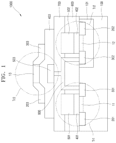
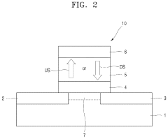
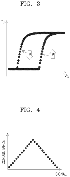
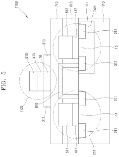
Semiconductor device including ferroelectric material, neuromorphic circuit including the semiconductor device, and neuromorphic computing apparatus including the neuromorphic circuit
PatentActiveUS11887989B2
Innovation
- The development of semiconductor devices and neuromorphic circuits incorporating ferroelectric materials, which enable efficient data processing by simulating synaptic functions, allowing for parallel processing and improved data storage and retrieval, thereby enhancing the accuracy and speed of data processing.
Multi-state device based on ion trapping
PatentWO2019106475A1
Innovation
- A semiconductor structure incorporating a non-volatile battery with a multi-state analog memory device, featuring a battery stack with specific layers such as cathode and anode current collectors, ion diffusion barriers, and an electrolyte, which improves output voltage retention and voltage resolution, enabling enhanced performance in neuromorphic computing.
Energy Efficiency Comparison Across Computing Paradigms
Neuromorphic computing systems based on semiconductor materials demonstrate remarkable energy efficiency advantages compared to traditional computing paradigms. When examining power consumption metrics, semiconductor-based neuromorphic chips typically operate in the milliwatt range, while conventional CPUs require several watts to tens of watts for comparable computational tasks. This translates to energy savings of approximately 2-3 orders of magnitude in many applications, particularly those involving pattern recognition and sensory processing.
The fundamental efficiency advantage stems from the event-driven nature of neuromorphic architectures. Unlike traditional von Neumann architectures that continuously consume power regardless of computational load, semiconductor neuromorphic systems activate circuits only when processing spikes or events, significantly reducing static power consumption. For instance, IBM's TrueNorth neuromorphic chip achieves 46 billion synaptic operations per second per watt, compared to approximately 2-5 billion operations per watt in high-performance GPUs.
When comparing across different computing paradigms, the energy efficiency hierarchy typically follows: traditional CPUs (least efficient), GPUs, FPGAs, ASICs, and neuromorphic chips (most efficient). Semiconductor-based neuromorphic systems demonstrate particular efficiency in tasks requiring temporal processing and sparse activations. For example, SpiNNaker systems have shown 50-100x energy improvements for certain neural network implementations compared to GPU implementations.
The efficiency advantage becomes even more pronounced when considering the energy per synaptic operation metric. While conventional digital systems require approximately 10-100 picojoules per operation, semiconductor neuromorphic implementations can achieve femtojoule-level efficiency. Intel's Loihi neuromorphic research chip demonstrates this advantage with energy consumption as low as 23-1000x less than conventional architectures when running equivalent workloads.
From a theoretical perspective, the human brain—the ultimate neuromorphic system—operates at approximately 20 watts while performing computations that would require megawatts in conventional computing systems. While semiconductor neuromorphic systems haven't yet reached biological efficiency levels, they represent the closest computational paradigm to this ideal. Current research indicates potential for further efficiency improvements of 1-2 orders of magnitude through advanced semiconductor materials and novel circuit designs.
The energy efficiency advantage of semiconductor neuromorphic systems becomes particularly critical in edge computing applications where power constraints are severe. In these scenarios, the ability to perform complex sensory processing and inference tasks at milliwatt power levels enables entirely new categories of intelligent devices that would be impractical with conventional computing approaches.
Alternative Materials Research for Next-Generation Neural Hardware
While silicon-based semiconductors currently dominate neuromorphic computing, researchers are actively exploring alternative materials that could potentially overcome existing limitations and enable more efficient brain-like computing systems. These alternative materials offer unique properties that may better mimic biological neural functions or provide superior performance characteristics for specific neuromorphic applications.
Phase-change materials (PCMs) represent one promising direction, utilizing their ability to rapidly switch between amorphous and crystalline states to store information. Materials like germanium-antimony-tellurium (GST) compounds demonstrate excellent scalability and multi-level resistance states, making them suitable for implementing synaptic plasticity in artificial neural networks. Recent research has shown PCM-based neuromorphic devices achieving energy consumption as low as femtojoules per synaptic event.
Memristive oxide materials, including hafnium oxide, tantalum oxide, and various transition metal oxides, exhibit resistance switching behaviors analogous to biological synapses. These materials can maintain their resistance state without power consumption, offering significant advantages for energy efficiency. Their compatibility with CMOS fabrication processes also makes them attractive candidates for large-scale integration.
Organic and bio-inspired materials represent another frontier in neuromorphic hardware development. Conducting polymers and organic semiconductors can operate at lower voltages than traditional semiconductors and potentially interface directly with biological systems. Some research groups have demonstrated artificial synapses using protein-based materials that closely mimic biological neural functions while consuming minimal power.
Two-dimensional (2D) materials such as graphene, molybdenum disulfide, and hexagonal boron nitride offer exceptional electrical properties at atomic-scale thicknesses. Their unique quantum properties and extreme thinness enable novel device architectures that could dramatically reduce the size and energy consumption of neuromorphic systems. Recent experiments with graphene-based memristive devices have shown promising results for spike-timing-dependent plasticity implementation.
Spintronic materials, which leverage electron spin rather than charge for information processing, may enable ultra-low-power neuromorphic computing. Magnetic tunnel junctions and skyrmion-based devices can implement synaptic and neuronal functions with minimal energy dissipation. These technologies could potentially operate at speeds exceeding conventional semiconductor approaches while consuming orders of magnitude less power.
The development of these alternative materials faces significant challenges, including manufacturing scalability, long-term stability, and integration with existing semiconductor infrastructure. However, their potential benefits in terms of energy efficiency, processing speed, and biological mimicry make them crucial research areas for advancing next-generation neuromorphic computing systems.
Unlock deeper insights with PatSnap Eureka Quick Research — get a full tech report to explore trends and direct your research. Try now!
Generate Your Research Report Instantly with AI Agent
Supercharge your innovation with PatSnap Eureka AI Agent Platform!