Inverse slope isolation and dual surface orientation integration

a technology of slope isolation and orientation integration, applied in the field of field effect transistors, can solve the problems of non-uniform silicon step/recess height between the different crystal surfaces, affecting device performance, and adding significant cost and complexity to the device fabrication

US20080268587A1Inactive Publication Date: 2008-10-30NXP USA INC
11 Cites 41 Cited by

Patent Information

Authority / Receiving Office
US · United States
Patent Type
Applications(United States)
Current Assignee / Owner
Publication Date
2008-10-30
Estimated Expiration
Not applicable · inactive patent

Smart Images

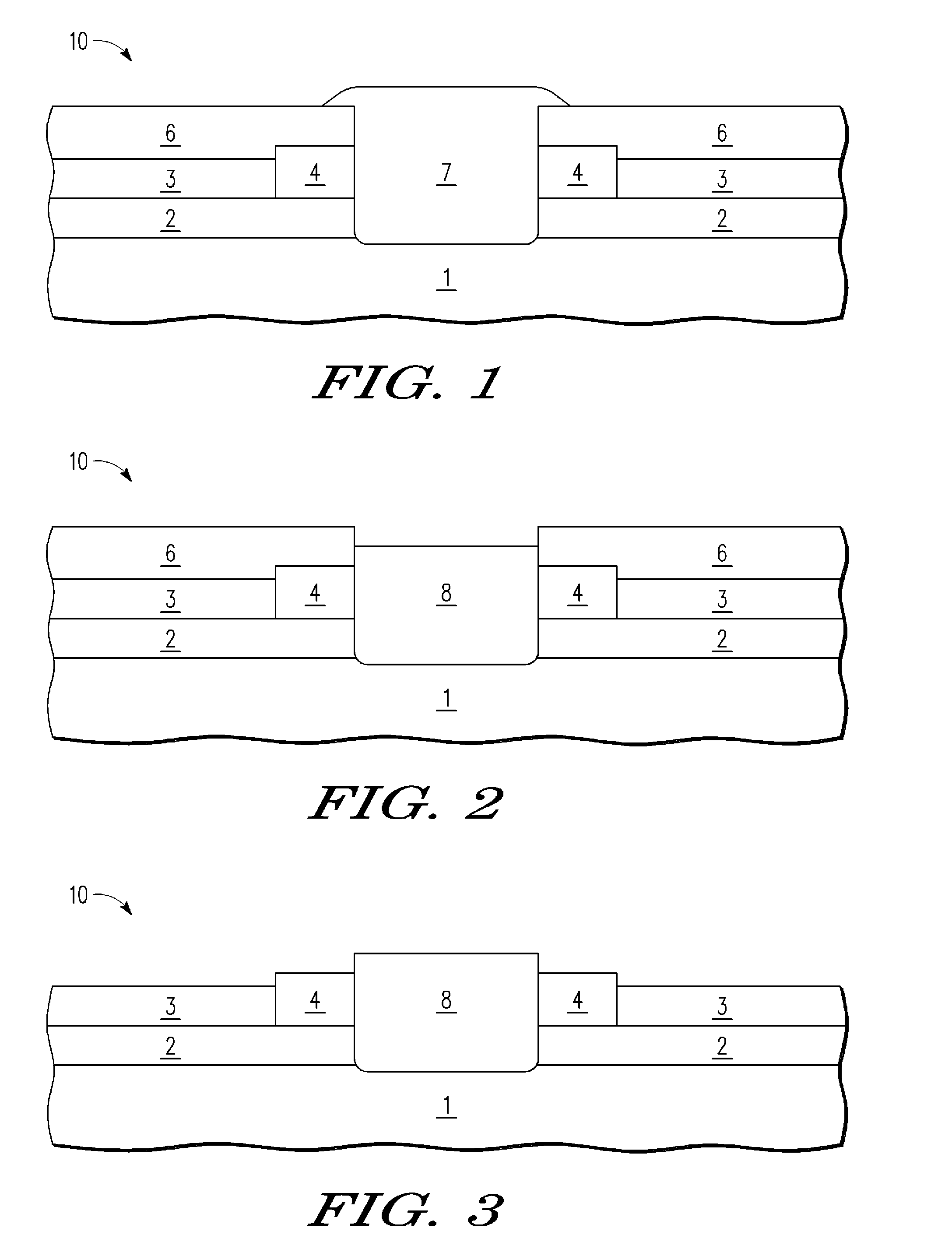
  • Figure 1
    Figure 1
  • Figure 2
    Figure 2
  • Figure 3
    Figure 3
Patent Text Reader

Abstract

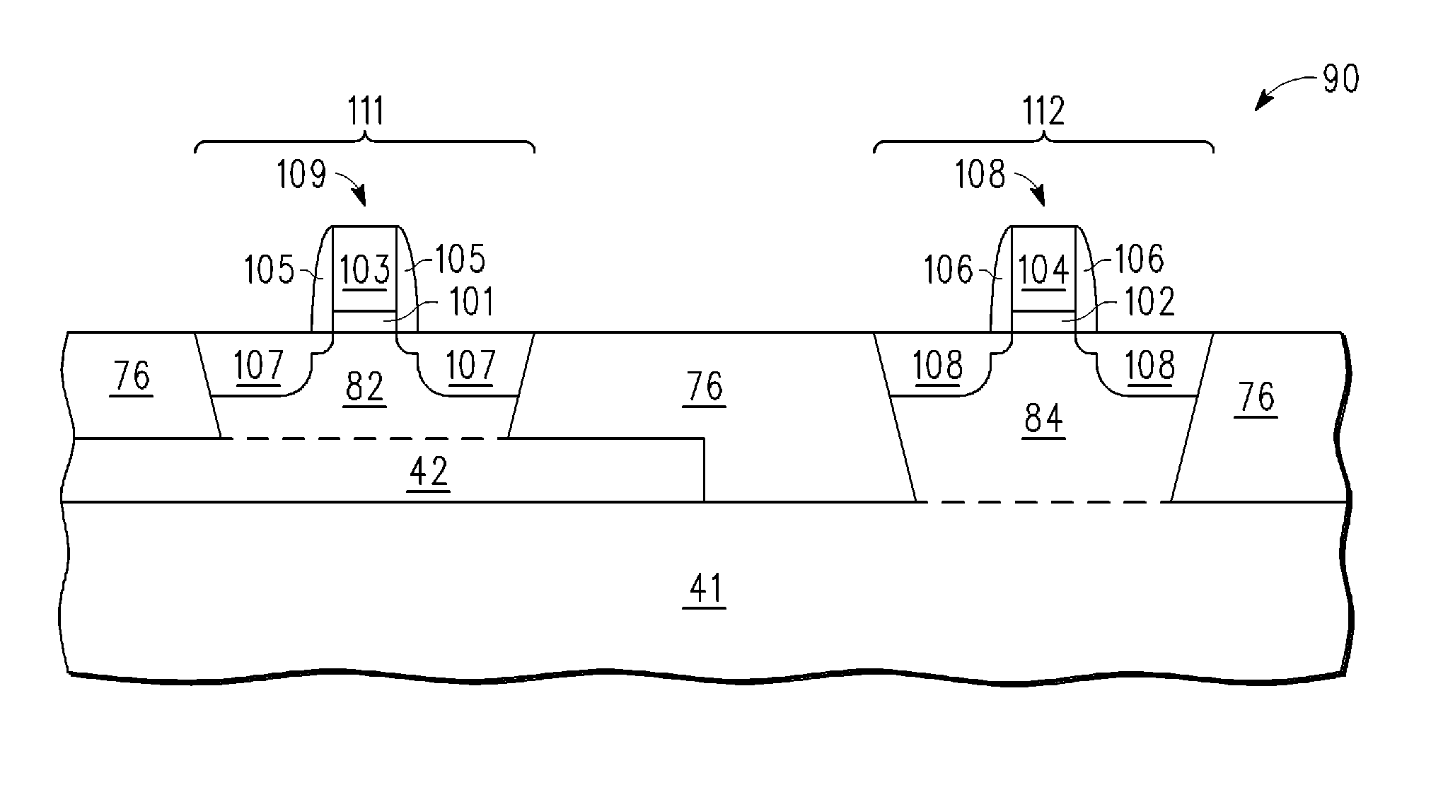
A semiconductor process and apparatus provide a high performance CMOS devices (108, 109) with hybrid or dual substrates by etching a deposited oxide layer (62) using inverse slope isolation techniques to form tapered isolation regions (76) and expose underlying semiconductor layers (41, 42) in a bulk wafer structure prior to epitaxially growing the first and second substrates (84, 82) having different surface orientations that may be planarized with a single CMP process. By forming first gate electrodes (104) over a first substrate (84) that is formed by epitaxially growing (100) silicon and forming second gate electrodes (103) over a second substrate (82) that is formed by epitaxially growing (110) silicon, a high performance CMOS device is obtained which includes high-k metal PMOS gate electrodes having improved hole mobility.
Need to check novelty before this filing date? Find Prior Art

Description

BACKGROUND OF THE INVENTION

[0001] 1. Field of the Invention

[0002] The present invention is directed in general to the field of semiconductor devices. In one aspect, the present invention relates to field effect transistors (FETs) fabricated on hybrid or dual substrates.

[0003] 2. Description of the Related Art

[0004] To address the difference in electron and hole mobility values for NMOS and PMOS transistor devices formed on semiconductor wafers having a single crystal orientation, CMOS devices are increasingly fabricated with hybrid substrates with different or dual surface orientations (DSO) using semiconductor-on-insulator (SOI) or bulk silicon wafer bonding to provide PMOS and NMOS devices with their own optimized crystal orientation. Prior attempts to integrate dual or hybrid substrates from a bonded SOI wafer have etched through the buried oxide layer to expose an underlying silicon layer which is used to epitaxially grow one of the crystal surface orientations, but have resulted in...

Examples

Embodiment Construction

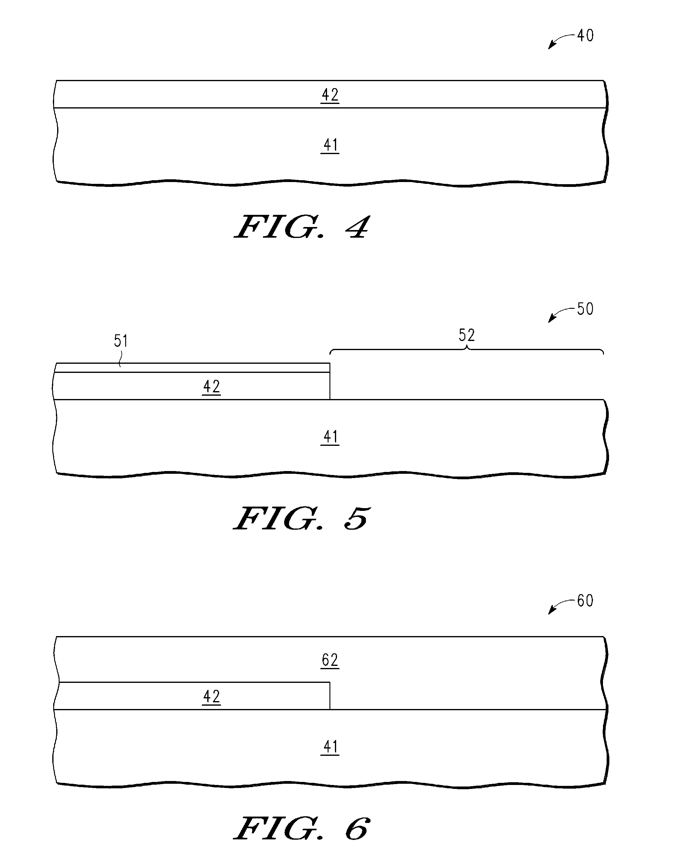
[0017]A method and apparatus are described for fabricating high performance CMOS devices with hybrid or dual substrates by etching a deposited dielectric layer to form tapered isolation regions and expose underlying semiconductor layers in a bulk wafer structure prior to epitaxially growing the first and second substrates having different surface orientations. Using an inverse slope isolation approach to define openings in the deposited dielectric layer that expose the underlying semiconductor layers, dual surface orientation (DSO) substrates can be epitaxially grown at the same time in a cost effective way that results in improved device performance and improved planarity for the first and second substrate heights. By improving the planarization of the dual substrate surfaces, better photolithography control is obtained and dispersion in device parametrics and performance is reduced. In addition, improved planarity in the substrate heights reduces non-uniformity due to variations i...