
High density inductor and method for producing same
a high density, inductor technology, applied in the direction of inductance, double resist layer, conductive pattern formation, etc., can solve the problems of inability to reduce the space between the wires of the coil, the inductance cannot be deeply oriented vertically, and the inductance cannot be reduced. , to achieve the effect of reducing the size of the core member enveloping the coil, forming a wire layer reliably, and reducing the thickness
- Summary
- Abstract
- Description
- Claims
- Application Information
AI Technical Summary
Benefits of technology
Problems solved by technology
Method used
Image

Examples
example
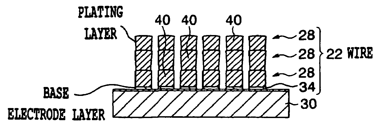
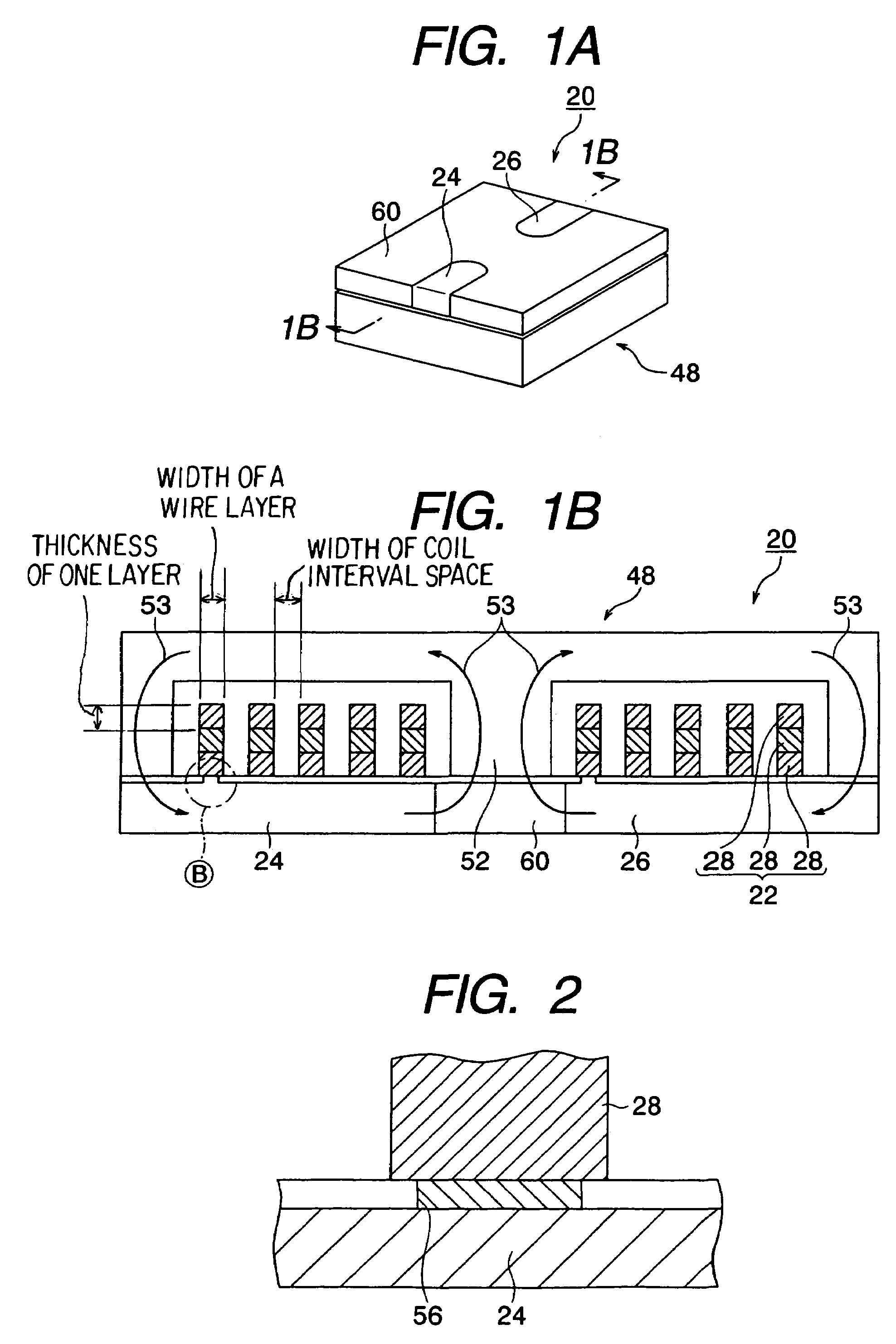
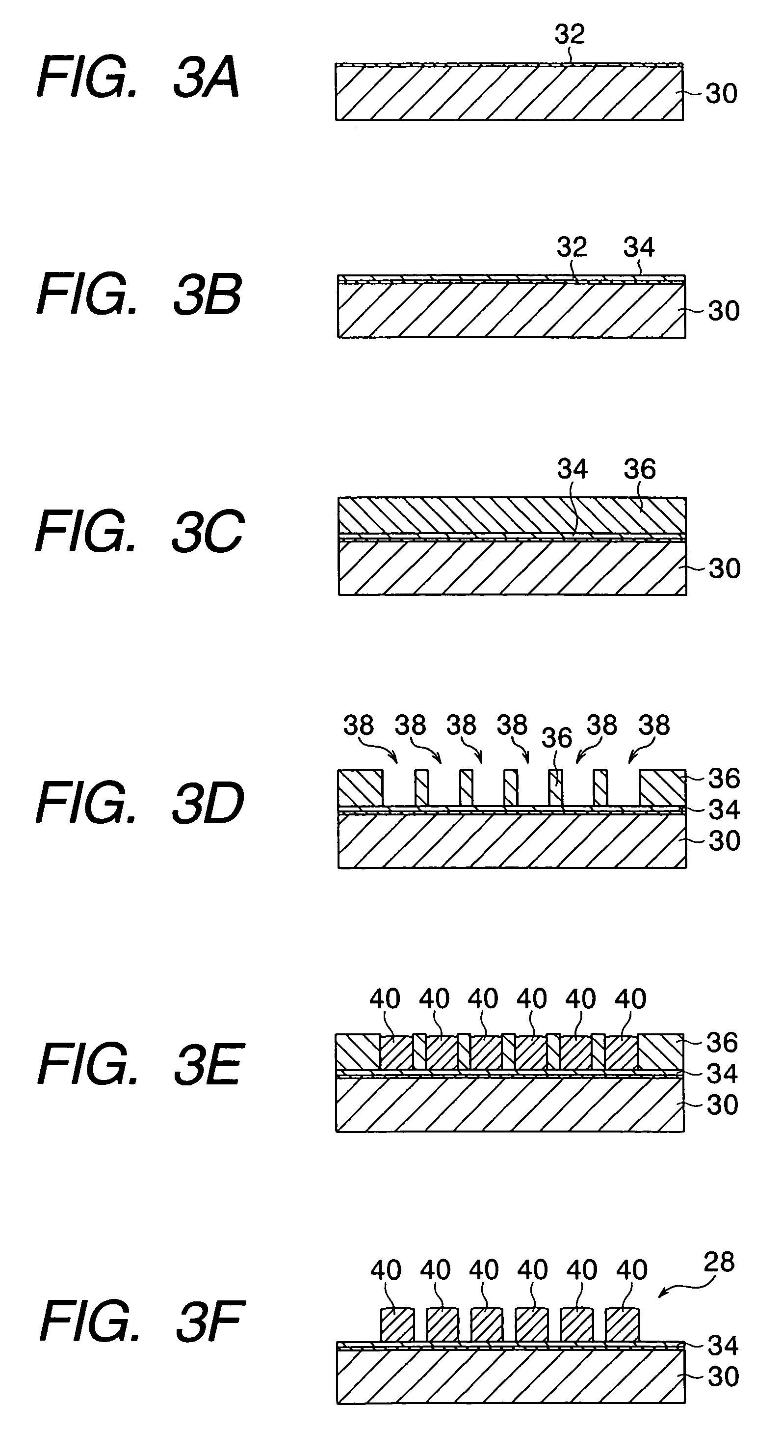
[0121]A coil pattern was formed on a substrate having a base conductive layer. For example in the case that a coil pattern with a thickness of the electroconductive portion of 40 μm and a width of the coil interval space of 10 μm is to be formed, the width of the resist pattern should be 10 μm. The allowable height for the resist of the aforementioned width with which the width of the resist will remain constant and the resist will not be bent is about 40 μm or less. In order to ensure the resolution realizing a resist width of 10±2 μm in both the upper and lower portions of the pattern, exposure light having a wavelength of 360 nm was used.
[0122]With the above conditions, the first layer of the coils with the coil width of 40 μm and a spacing of 10 μm was formed.
[0123]At that time, all of the coils of the first layer were normally formed on the substrate without being bent, in other words the process yield was 100%.
[0124]Next, a pattern of the second layer was formed on top of the ...
PUM
| Property | Measurement | Unit |
|---|---|---|
| height | aaaaa | aaaaa |
| height | aaaaa | aaaaa |
| thickness | aaaaa | aaaaa |
Abstract
Description
Claims
Application Information