
Dry etching method for removing silicon nitride film
A technology of silicon nitride thin film and dry etching, which is applied in the direction of electrical components, semiconductor/solid-state device manufacturing, circuits, etc., can solve the problems of affecting the electrical performance of semiconductor devices, damage, and the inability to deposit gate oxide layers, etc., to achieve reduction The chance of bombardment, reducing the severity, and reducing the effect of potential difference
Patent Information
- Authority / Receiving Office
- CN · China
- Patent Type
- Patents(China)
- Current Assignee / Owner
- Publication Date
- 2011-10-05
- Estimated Expiration
- Not applicable · inactive patent
Smart Images
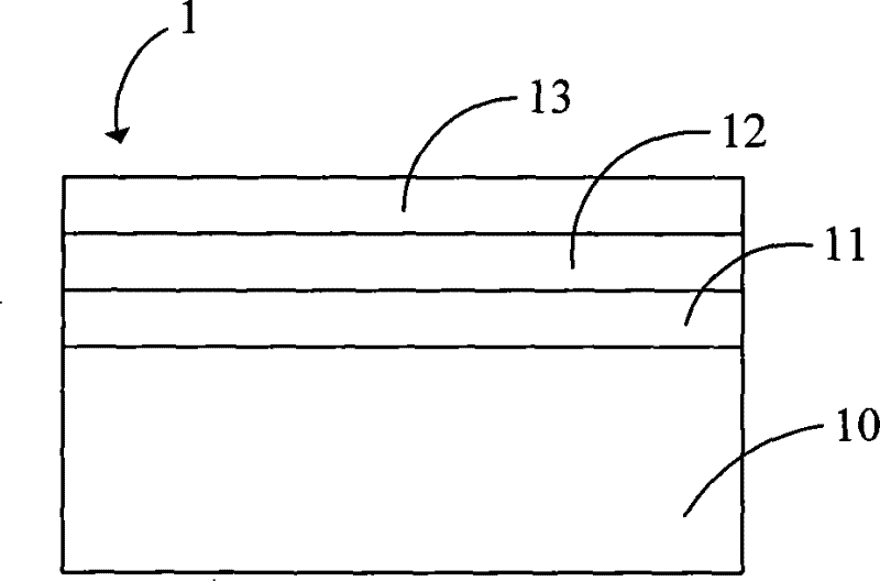
Figure 1 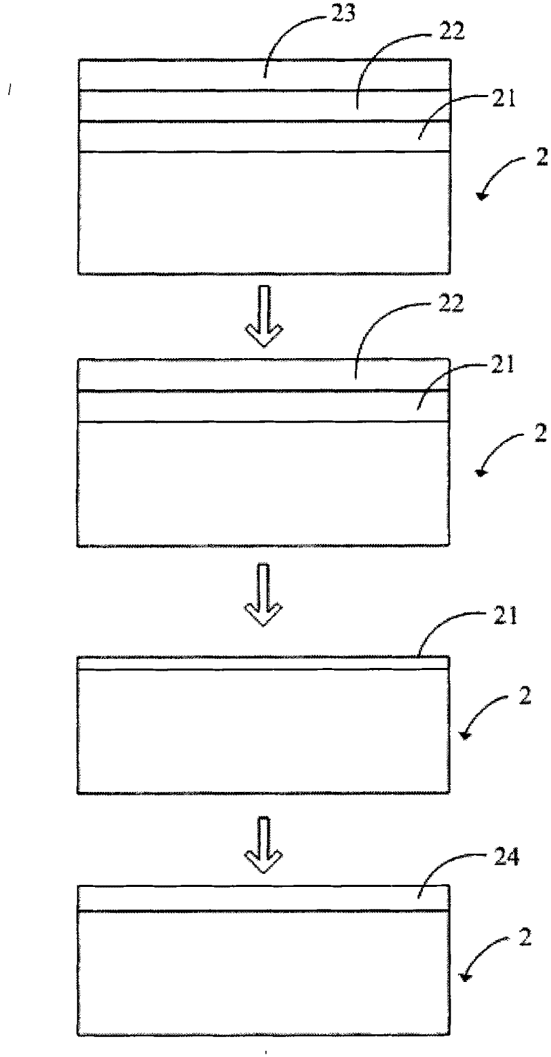
Figure 2
Abstract
Description
technical field
[0001] The invention relates to a dry etching method for manufacturing a semiconductor non-volatile memory device, in particular to a dry etching method for removing a silicon nitride film. Background technique
[0002] Flash memory is a non-volatile memory that can store charge even when the system is powered off. The storage unit of the flash memory is a MOS tube, but its structure is slightly different from that of a general MOS tube. The structure of the flash MOS tube is as follows figure 1 As shown, the structure of the flash memory MOS transistor region 1 includes a silicon substrate 10, a gate oxide layer 11, a floating gate 12, an inter-electrode oxide layer 13 and a control gate (not shown) from bottom to top. The floating gate 12 is made of silicon nitride (Si 3 N 4 ) film to store charge. Both the gate oxide layer 11 and the inter-electrode oxide layer 13 are silicon dioxide (SiO 2 )film.
[0003] Generally, a variety of semiconductor devic...
Examples
Embodiment Construction
[0010] One embodiment of the dry etching method for removing silicon nitride film provided by the present invention will be described in detail below with reference to the accompanying drawings, in order to further understand the technical scheme, purpose and beneficial effects of the invention. . see figure 2 For the sake of concise description, in this embodiment, the etching of the silicon nitride film, the oxide film where the gate oxide and the inter-electrode oxide are located is referred to as the ONO etching process.
[0011] The dry etching method provided by the invention is applied in the ONO etching process. The dry etching method is used to remove the silicon nitride film 22 in the non-flash MOS tube region, and is performed in a process chamber. The upper and lower sides of the plasma region of the processing chamber have an upper substrate and a lower substrate. The upper plate is connected to the source power to excite the gas input into the process chamber...