
Groove-type Schottky diode and manufacture method thereof
A technology of Schottky diodes and manufacturing methods, applied in semiconductor/solid-state device manufacturing, electrical components, circuits, etc., can solve problems such as fault generation and easy faults, and achieve short reverse recovery time and low reverse voltage leakage current , excellent structural effect
Patent Information
- Authority / Receiving Office
- CN · China
- Patent Type
- Patents(China)
- Current Assignee / Owner
- Publication Date
- 2011-05-25
Smart Images
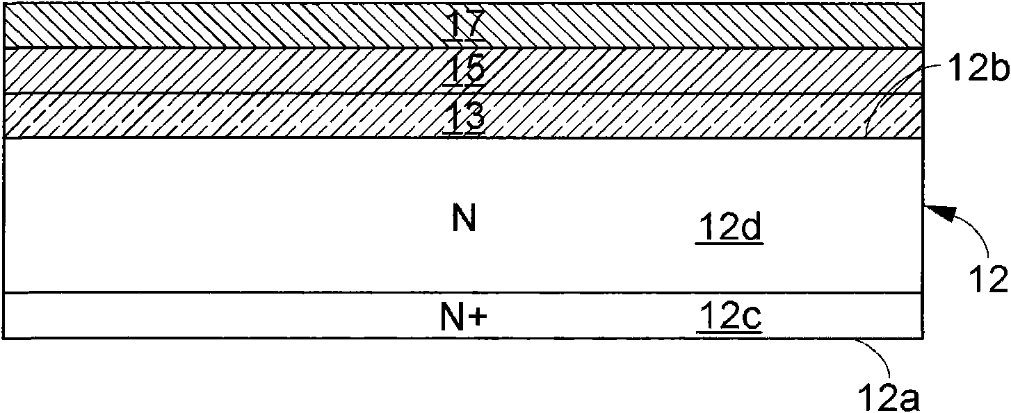
Figure 1 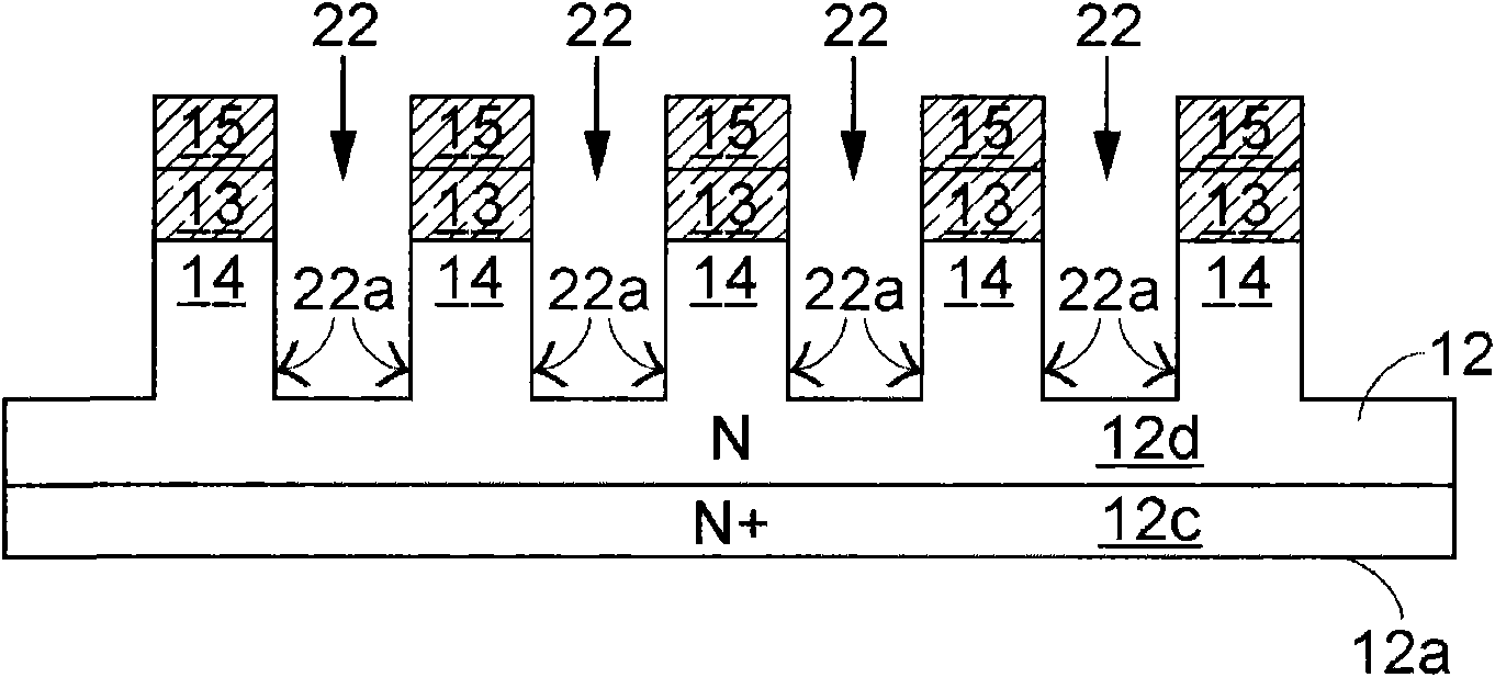
Figure 2 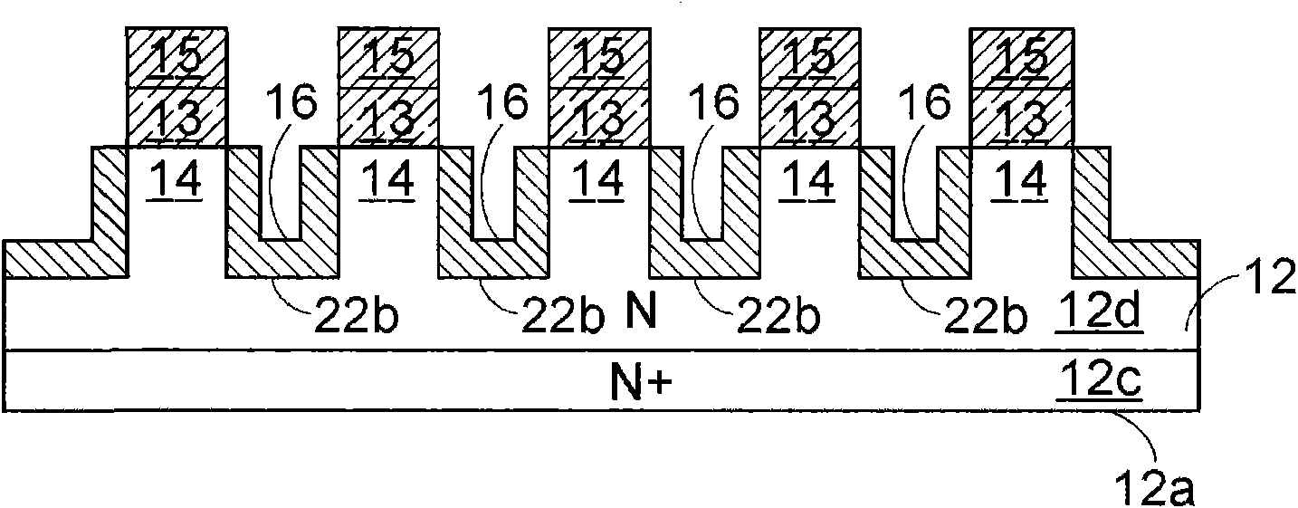
Figure 3
Abstract
Description
Technical field
[0001] The present invention relates to a trench type Schottky diode and a manufacturing method thereof, in particular to a manufacturing method to provide a lower reverse voltage leakage current, lower forward bias voltage (Vf), and Trench Schottky diode with high reverse withstand voltage and short reverse recovery time (tRR). Background technique
[0002] Schottky Diode (Schottky Diode) is a unipolar element that uses electrons as carriers. It is characterized by fast speed and can be used when a lower forward bias voltage (Vf) is added. There is a larger forward current and a shorter reverse recovery time (Reverse Recovery Time; tRR), but if a continuously increasing reverse bias voltage is added, there will be a larger leakage current (with metal work function and semiconductor Schottky barrier caused by doping concentration (Schottky Barrier). Afterwards, the trench-type Schottky barrier diode was proposed. By filling the trench with polysilicon or metal t...
Examples
Embodiment Construction
[0029] See Figure 2(a) to Figure 2(o) , Is a schematic diagram of the manufacturing process of the preferred embodiment of the trench-type Schottky diode manufacturing method proposed by the present invention. As shown in Figure 2(a), first, a semiconductor substrate 30 is provided; in this embodiment, the semiconductor substrate 30 includes a silicon substrate 31 with a high doping concentration (N+ type) and a low doping concentration (N Type) epitaxial layer 32; and the low doping concentration epitaxial layer 32 is formed on the high doping concentration silicon substrate 31, and the low doping concentration epitaxial layer 32 has a certain thickness to provide the Invented the subsequent formation of the multi-trench structure (Multi-Trench) by etching.
[0030] Then, a thermal oxidation process is performed on the surface 32a of the semiconductor substrate 30, that is, the surface 32a where the epitaxial layer 32 with low doping concentration is located, and then on the s...