
Pixel substrate and fabrication method thereof, LCD( liquid crystal display) panel and LCD device
A substrate and liquid crystal layer technology, applied in static indicators, semiconductor/solid-state device manufacturing, optics, etc., can solve the problems of inability to transmit light, reduce the display quality of the multi-domain vertical alignment liquid crystal display panel 202, and the liquid crystal molecules 132 topple over, etc. , to achieve good display quality, less dark lines, less dark lines
Patent Information
- Authority / Receiving Office
- CN · China
- Patent Type
- Patents(China)
- Current Assignee / Owner
- Publication Date
- 2015-04-01
- Estimated Expiration
- Not applicable · inactive patent
Smart Images
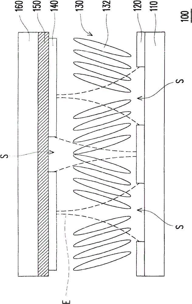
Figure 1 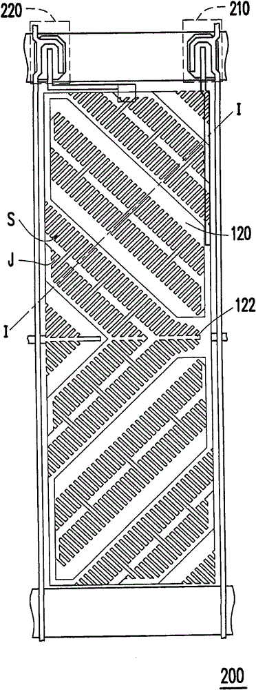
Figure 2 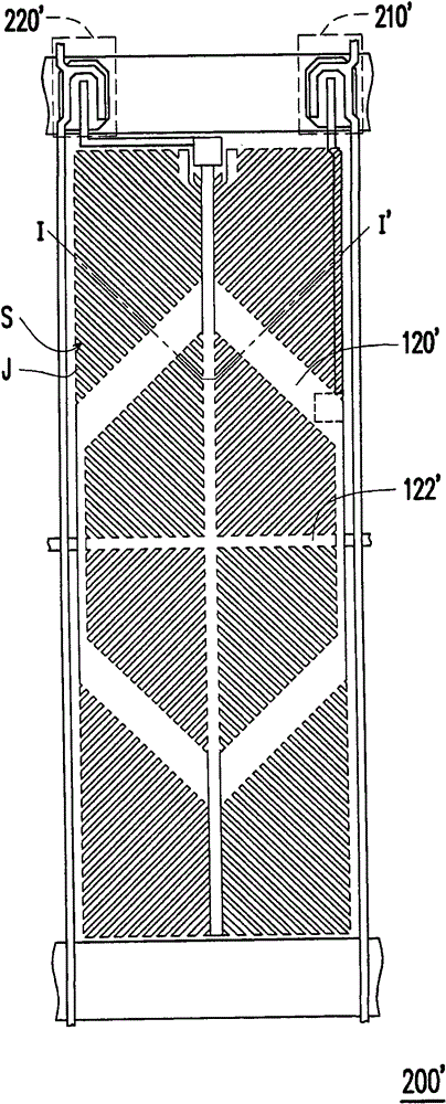
Figure 3
Abstract
Description
technical field
[0001] The present invention relates to a substrate with a pixel structure and a manufacturing method thereof, a liquid crystal display panel and a liquid crystal display device having the substrate, and in particular to a low color shift (Low Color Shift, LCS) and dark grain A few substrates with a multi-domain vertical alignment (MVA) pixel structure and a manufacturing method thereof, as well as a liquid crystal display panel and a liquid crystal display device having the same. Background technique
[0002] Liquid crystal display has superior characteristics such as high image quality, good space utilization efficiency, low power consumption, and no radiation. At present, the following liquid crystal displays with good display effects are proposed, such as: in-plane switching (IPS) liquid crystal display, fringe field switching (FFS) liquid crystal display, multi-domain vertical alignment (multi-domain vertical alignment, MVA) liquid crystal display, and ...
Examples
no. 1 example
[0136] Figure 4 It is a schematic top view of a substrate with a multi-domain vertical alignment pixel structure according to a preferred embodiment of the present invention. Figure 5A for Figure 4 The cross-sectional schematic diagram of the multi-domain vertically aligned pixel structure along the line A-A'. Figure 5B for Figure 5A There is an equivalent circuit diagram of the membrane layer with applied voltage in .
[0137] Please also refer to Figure 4 , Figure 5A and Figure 5B , the substrate 310 with 300 can be opposite to the opposite substrate 384 with the common electrode 380 , and the liquid crystal layer 390 is located between the substrate 310 and the opposite substrate 384 . The substrate 310 includes: a scan line 320 , a data line 330 , an active element 340 , a first patterned pixel electrode 350 , a voltage drop layer 370 and a second patterned pixel electrode 360 . The scan lines 320 and the data lines 330 divide the substrate 310 into a plur...
no. 2 example
[0195] In addition, in order to improve the resolution of the current exposure machine and the etching process capability, the process width limit is 3.5 μm, and the width of the elongated pixel electrode pattern J cannot be effectively increased. Therefore, in Figure 13A In the pixel structure 700 of the embodiment, two layers of patterned pixel electrodes are used, and the strip electrodes of the two layers of patterned pixel electrodes are offset by a certain distance from each other, so as to increase the width of the strip electrodes equivalently to solve the problem of The dark fringe phenomenon caused by the low electric field intensity at the slit is further detailed as follows.
[0196] Figure 13A It is a schematic top view of another substrate with a multi-domain vertical alignment pixel structure according to a preferred embodiment of the present invention. Figure 13B for Figure 13A The cross-sectional schematic diagram of the multi-domain vertical alignment p...
no. 3 example
[0208] In addition, to improve image 3 In view of the problem of dark lines in the multi-domain vertical alignment type liquid crystal display panel 202, the present invention proposes another substrate 810 having another multi-domain vertical alignment type pixel structure 800, which will be described in detail below.
[0209] Figure 15A It is a schematic top view of another substrate with a multi-domain vertical alignment pixel structure according to a preferred embodiment of the present invention. Figure 15B for Figure 15A The cross-sectional schematic diagram of the multi-domain vertical alignment pixel structure along the line II-II'. Figure 15C for Figure 15A The cross-sectional schematic diagram of the multi-domain vertical alignment pixel structure along the line III-III'. from Figure 15B It can be known that the following first patterned pixel electrode 875 is connected to the bias electrode 850 (equal voltage), from Figure 15C The distribution of the el...