
White-light LED (light-emitting diode) chip structure with self-assembly nano structure
A technology of LED chips and nanostructures, which is applied to electrical components, circuits, semiconductor devices, etc., can solve the problems of low light extraction efficiency of light-emitting diodes, achieve low resistance, increase the probability of light emission, and high transmittance. Effect
Patent Information
- Authority / Receiving Office
- CN · China
- Patent Type
- Applications(China)
- Current Assignee / Owner
- Publication Date
- 2012-10-17
- Estimated Expiration
- Not applicable · inactive patent
Smart Images
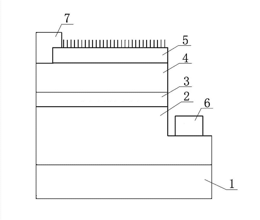
Figure 1 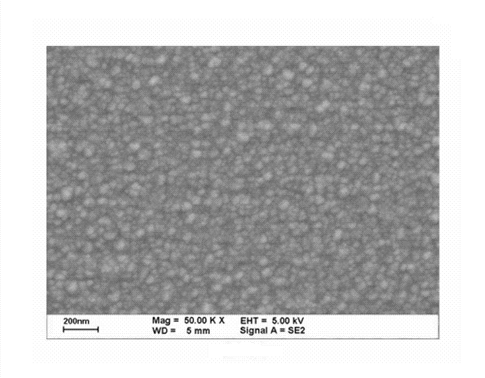
Figure 2 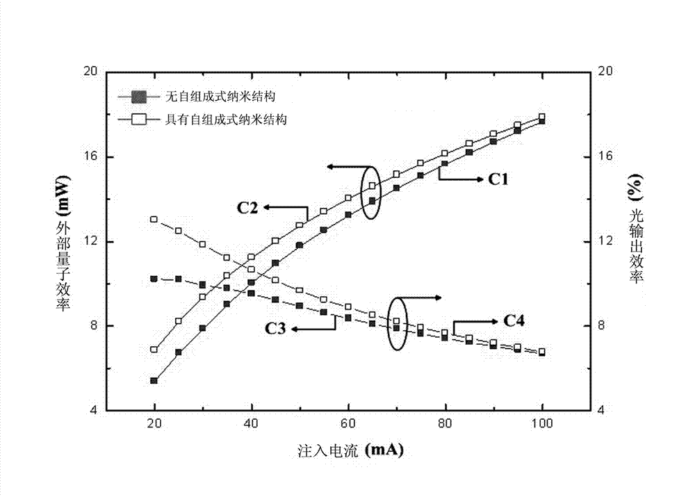
Figure 3
Abstract
Description
technical field
[0001] The invention relates to a light-emitting diode assembly, in particular to a white LED chip structure with a self-assembled nanostructure. Background technique
[0002] A light-emitting diode is a solid-state semiconductor component made of various compound semiconductor materials. It can emit various colors of visible light or invisible light such as infrared rays and ultraviolet rays according to the energy gap characteristics of different materials. Wherein, the white light emitted by the white light emitting diode is mixed light formed by mixing color lights of at least two wavelengths. The chip structure of the existing white light emitting diode includes a sapphire substrate, an N-type GaN epitaxial layer, a multilayer quantum well InGaN active layer, a P-type GaN epitaxial layer, a negative electrode metal layer, and a positive electrode metal layer. Its working principle is: when the negative electrode metal layer and the positive electrode me...
Examples
Embodiment Construction
[0011] White light LED chip structure with self-organized nanostructure, including sapphire substrate 1, N-type GaN epitaxial layer 2, multi-layer quantum well InGaN active layer 3, P-type GaN epitaxial layer 4, negative electrode metal Layer 6, and positive electrode metal layer 7; also includes indium zinc oxide transparent conductive layer 5 with a self-organized nanostructure; wherein, N-type gallium nitride epitaxial layer 2 is stacked on sapphire substrate 1; multilayer quantum well nitrogen The InGaN active layer 3 is stacked on the N-type GaN epitaxial layer 2, and the N-type GaN epitaxial layer 2 is partially exposed outside the multilayer quantum well InGaN active layer 3; the P-type GaN epitaxial layer 4 is stacked on the multilayer quantum well indium gallium nitride active layer 3; the indium zinc oxide transparent conductive layer 5 with a self-constituted nanostructure is stacked on the p-type gallium nitride epitaxial layer 4, and the p-type gallium nitride epit...