
Manufacture method of semiconductor device
A manufacturing method and semiconductor technology, applied in the fields of semiconductor/solid-state device manufacturing, semiconductor devices, electric solid-state devices, etc., can solve problems such as indeterminacy, and achieve the effects of preventing the introduction of thermal strain, prolonging failure life, and high reliability.
Patent Information
- Authority / Receiving Office
- CN · China
- Patent Type
- Applications(China)
- Current Assignee / Owner
- Publication Date
- 2012-12-26
Smart Images
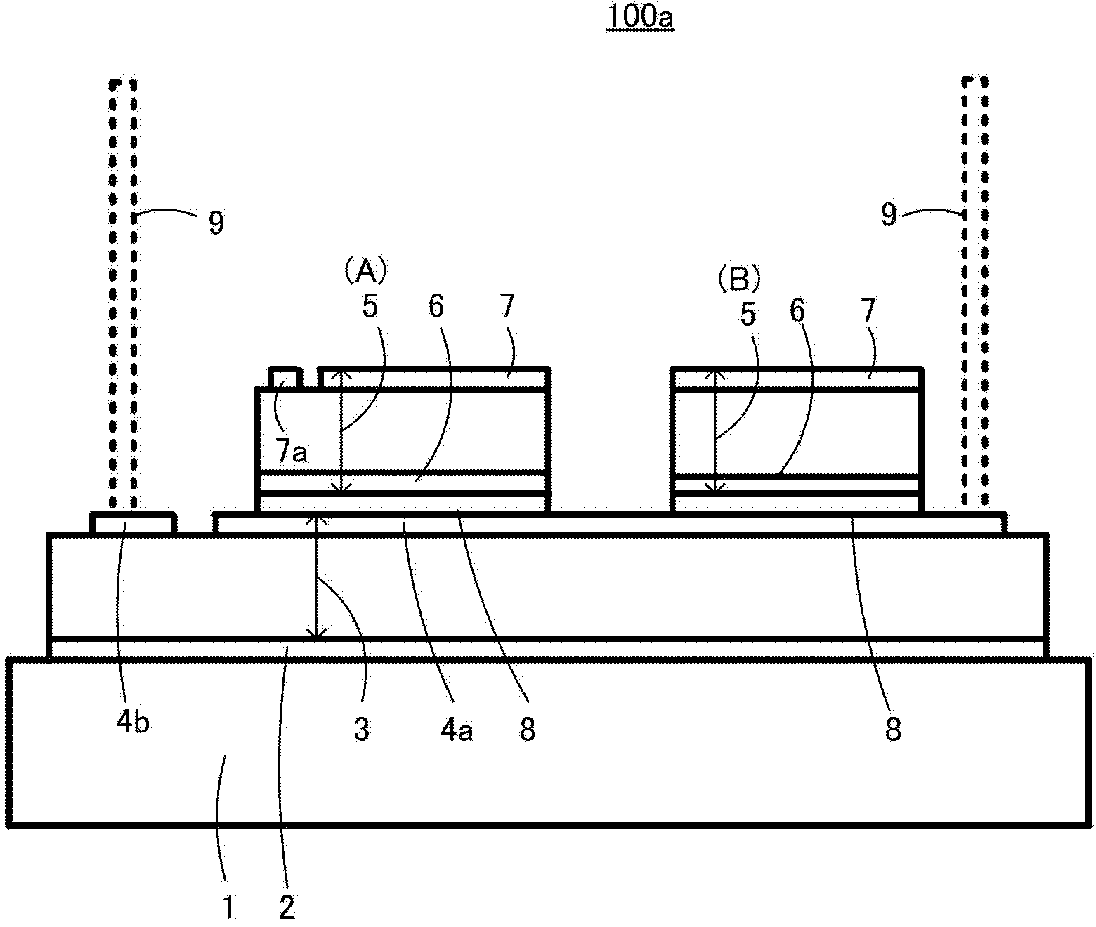
Figure 1 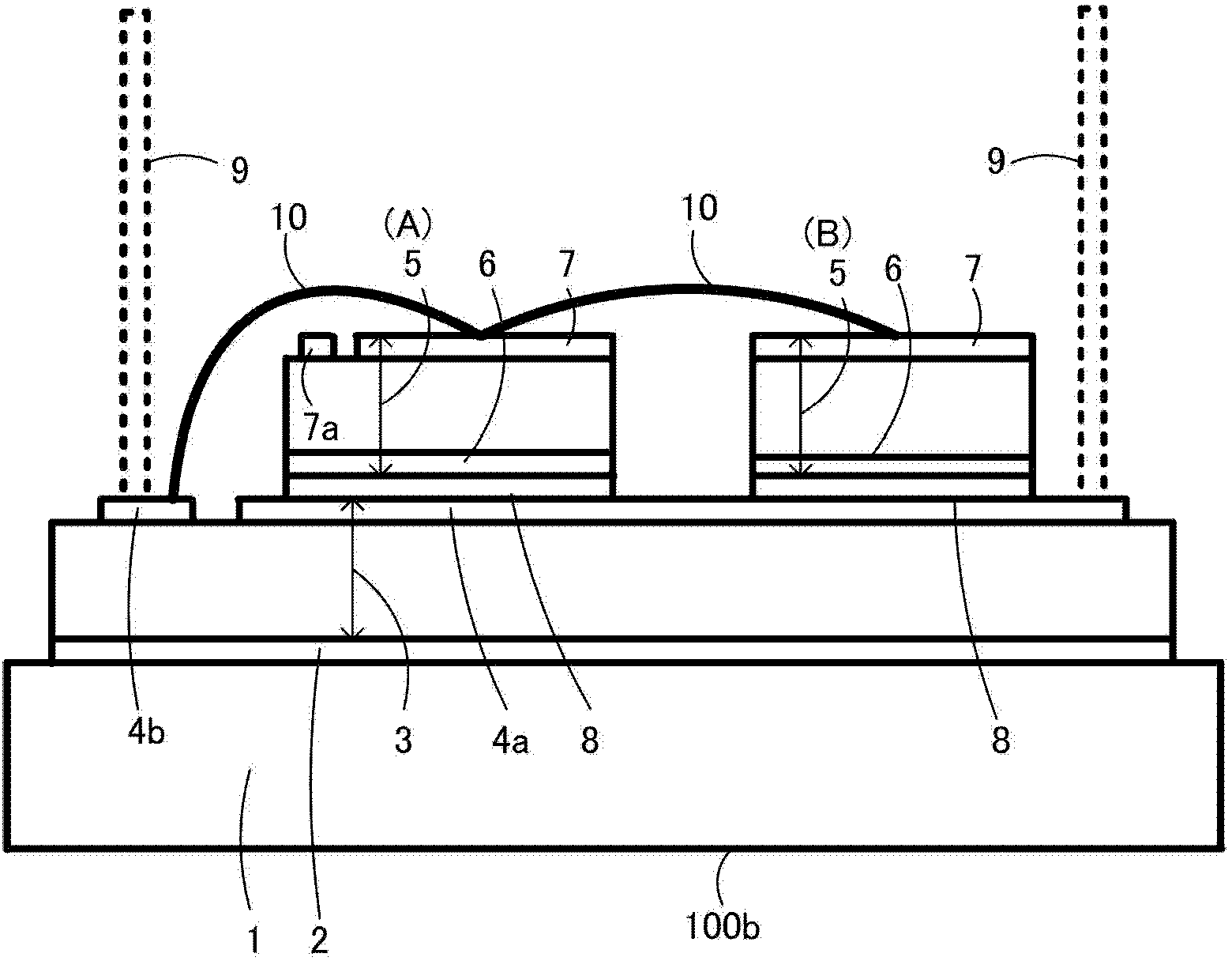
Figure 2 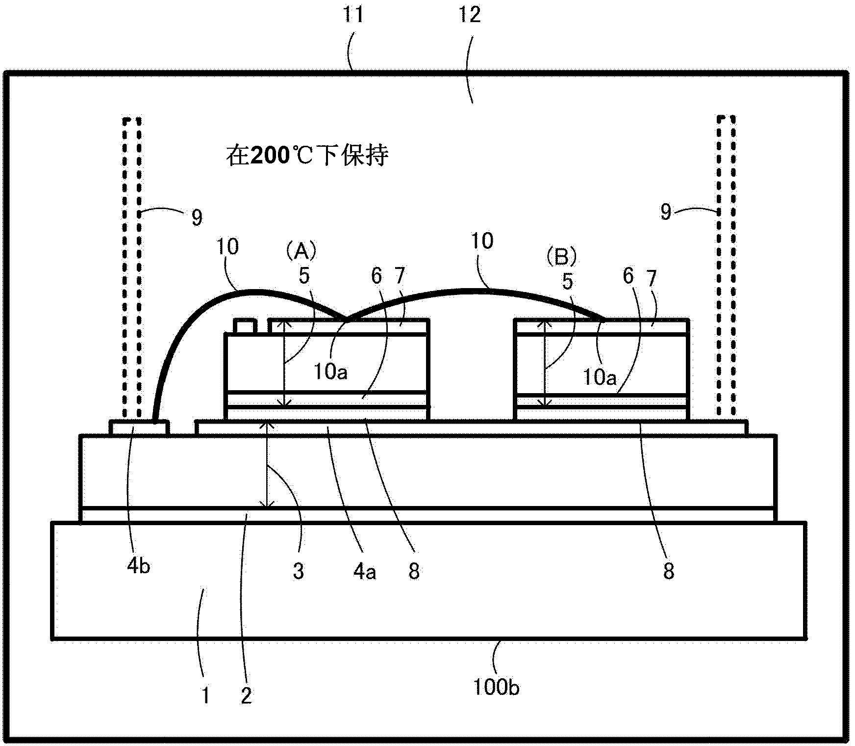
Figure 3
Abstract
Description
technical field
[0001] The invention relates to a method for manufacturing a semiconductor device, in particular to a method for bonding metal wires to surface electrodes of a semiconductor chip. Background technique
[0002] In recent years, there has been a demand for downsizing and weight reduction of automotive instrument control devices and electric vehicle drive control devices. The drive control device uses a semiconductor device that switches a large current at high speed in order to obtain AC (power) for driving the motor from a DC power source such as a battery. In response to the increase in electric power, that is, the increase in the operating current of electronic components, aluminum is mainly used in the electrical connection between semiconductor chips in semiconductor devices, between semiconductor chips and insulating substrates with conductive patterns that are fastened to semiconductor chips, etc. Composition of tinsel.
[0003] Such semiconductor devi...
Examples
Embodiment Construction
[0064] Embodiments are illustrated in the following examples.
[0065]
[0066] Figure 1 to Figure 6 This is a method of manufacturing a semiconductor device according to an embodiment of the present invention, and is a cross-sectional view of a main part of the manufacturing process shown in step by step. The semiconductor device is, for example, a power module in which an IGBT chip and a diode are connected in antiparallel.
[0067] First, if figure 1 As shown, the back electrode 6 of the semiconductor chip 5 is fixed with the bonding material 8 on the conductive pattern 4 a of the insulating substrate 3 with the conductive pattern 3 on which the bonding material 2 is fixed on the heat dissipation base plate 1 . In addition, an external lead-out terminal 9 is fixed to the conductive pattern 4b. This component composed of the heat dissipation base plate 1 , the insulating substrate with conductive patterns 3 , the semiconductor chip 5 and the external lead-out terminal...