
Xenon difluoride gas-phase etching method for barrier layer
A technique for etching barrier layers and xenon difluoride, which is applied in the fields of electrical components, semiconductor/solid-state device manufacturing, circuits, etc., can solve problems such as excessive etching of the barrier layer 23, and achieve improved etching uniformity and good process effects , the effect of increasing the etching rate
Patent Information
- Authority / Receiving Office
- CN · China
- Patent Type
- Applications(China)
- Current Assignee / Owner
- Publication Date
- 2014-04-02
Smart Images
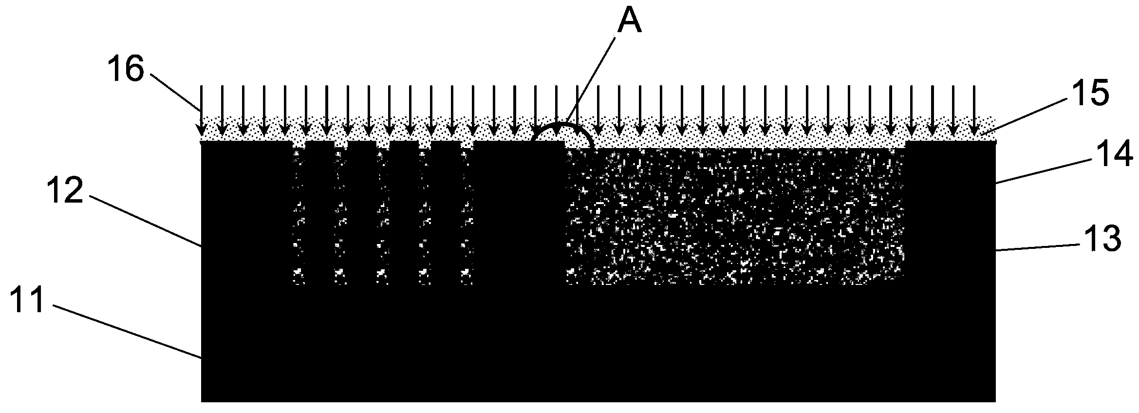
Figure 1 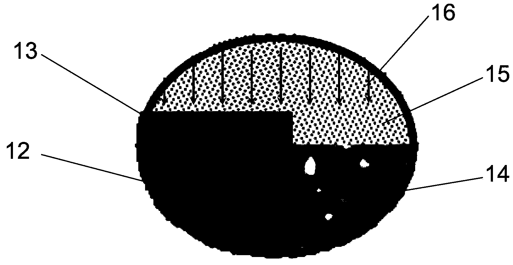
Figure 2 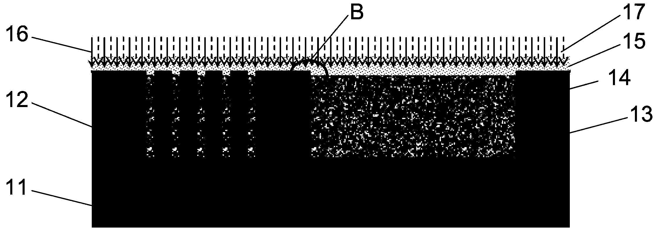
Figure 3
Abstract
Description
technical field
[0001] The invention relates to the technical field of integrated circuit device manufacturing, and more specifically, relates to a method for etching a barrier layer in the gas phase of xenon difluoride. Background technique
[0002] As the size of integrated circuit devices continues to shrink, interconnection delays have increasingly become a bottleneck problem restricting the development of integrated circuits. In order to reduce the interconnection delay, in the manufacture of metal interconnection lines of integrated circuit devices, metal copper with a lower resistivity is used instead of aluminum with a higher resistivity to reduce the interconnection resistance, and a low-K dielectric is selected. material to reduce the capacitance between metal interconnect lines. Such as Figure 6 and Figure 7 As shown, the manufacturing process of the metal interconnection generally includes: firstly, forming a low-K dielectric layer 22 on the semiconductor sub...
Examples
Embodiment Construction
[0024] In order to describe the technical content, achieved goals and effects of the present invention in detail, the following will be described in detail in conjunction with the embodiments and accompanying drawings.
[0025] The present invention relates to xenon difluoride (XeF 2 ) method of vapor phase etching barrier layer.
[0026] see figure 1 and figure 2 , is a schematic cross-sectional structure diagram of an embodiment of the xenon difluoride gas-phase etching barrier layer of the present invention, disclosing a method of the gas-phase etching barrier layer of xenon difluoride of the present invention. Before introducing the method for gas-phase etching barrier layer of xenon difluoride of the present invention in detail, the manufacturing process of the metal interconnection line is briefly introduced, including the following steps: first, a semiconductor substrate 11 is provided, and a low K dielectric layer 12; secondly, form trenches and connection holes o...