
Regulation control method for thin layer epitaxial transition region of heavily doped PH substrate
A transition zone and substrate technology, used in electrical components, semiconductor/solid-state device manufacturing, circuits, etc., can solve the problems of limited steepness in the transition zone, increased TCS flow, TCS waste, etc., to improve BVDS discreteness, increase Edge resistivity value, the effect of reducing the effect of self-doping
Patent Information
- Authority / Receiving Office
- CN · China
- Current Assignee / Owner
- Publication Date
- 2016-04-13
Smart Images
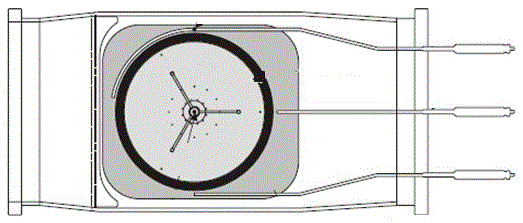
Figure 1 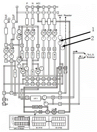
Figure 2 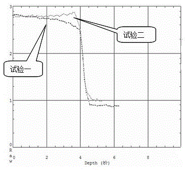
Figure 3
Abstract
Description
technical field
[0001] The invention relates to the technical field of growth methods of epitaxial layers, in particular to a method for regulating and controlling epitaxial transition regions of heavily doped pH substrate thin layers. Background technique
[0002] For the development of new epitaxial materials for low-voltage MOS devices on heavily doped PH substrates, the test results of resistivity (four-probe, 4PP test) are greatly affected by the transition region of the epitaxial layer. Delay, the lower the 4PP test result; for the general epitaxial process, the epitaxial resistivity can be adjusted by adjusting the dopant dose, the epitaxial thickness can be adjusted by the growth rate and growth time, and there is no general method for the epitaxial transition region. Adjustment. With the development of integrated circuits, the market demand for epitaxial materials for large-size low-voltage MOS devices is increasing. At present, the demand for epitaxial materials f...
Examples
Embodiment 1
[0029] The invention discloses a method for regulating and controlling a thin-layer epitaxial transition region of a heavily doped pH substrate, comprising the following steps:
[0030] 1) Fix the temperature and TCS (trichlorosilane) flow rate of the monolithic epitaxial growth system during the epitaxial growth of the substrate.
[0031] 2) During the epitaxial growth of the substrate, the growth of the CAP layer and the growth of the epitaxial layer use the same doping process.
[0032] 3) During the growth of the epitaxial layer, change the VENT (exhaust) pressure in the monolithic epitaxial growth system, so that the VENT pressure is greater than or less than the chamber (cavity) pressure of the system, and adjust the steepness of the epitaxial layer transition zone.
[0033] 4) By adjusting the VENT pressure, the steepness of the epitaxial layer transition zone is changed, and the corresponding epitaxial wafers are respectively analyzed for the extended resistance profil...
Embodiment 2
[0035] The invention discloses a method for regulating and controlling a thin-layer epitaxial transition region of a heavily doped pH substrate, comprising the following steps:
[0036] Using ASME2000 type monolithic epitaxial growth system, such as figure 1 As shown, the infrared lamp array is radiatively heated, the high-purity graphite base is a silicon wafer carrier, and the protective gas is ultra-high-purity H 2 Gas with a purity of over 99.999999%.
[0037] Using 8-inch heavily doped PH substrate, crystal orientation , resistivity range of 0.001-0.0015ohm.cm, supersealing back sealing process;
[0038] Before epitaxial growth, the system is fully removed from the doping treatment. At 1190 ° C, a large flow of HCL gas is introduced at 20 slm / min, and when the residual Si and the residual Si on the base are etched away, the H 2 The flow rate is set to 10slm / min, and when corroding the residual Si on the inner wall of the bell jar, increase the H 2 The flow rate is up t...