
Packaging structure and manufacturing method of a high-current power semiconductor device
A technology of power semiconductors and packaging structures, which is applied in semiconductor/solid-state device manufacturing, semiconductor devices, semiconductor/solid-state device components, etc. It can solve problems such as loss of resistance and thermal conductivity, virtual welding, frame deformation, etc., and achieve one-time The effect of processing and molding, simple process method, and reduced packaging resistance
Patent Information
- Authority / Receiving Office
- CN · China
- Patent Type
- Patents(China)
- Current Assignee / Owner
- Publication Date
- 2019-10-11
Smart Images
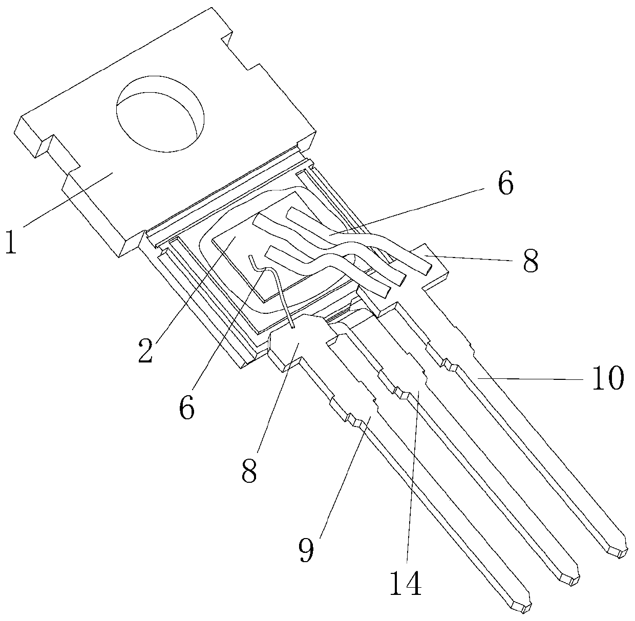
Figure 1 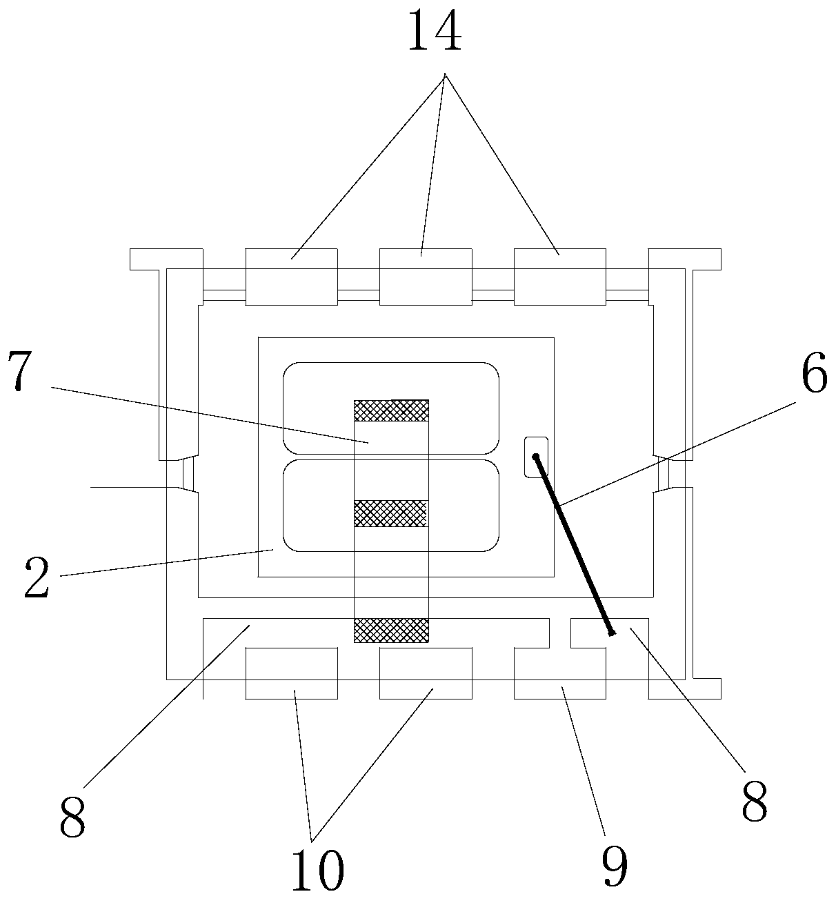
Figure 2 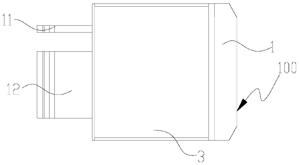
Figure 3
Abstract
Description
technical field
[0001] The invention relates to a packaging structure of a semiconductor device, in particular to a packaging structure of a high-current power semiconductor device, which belongs to the technical field of manufacturing semiconductor devices. Background technique
[0002] High-current and high-power semiconductor devices are constantly developing. Silicon-based trench semiconductor chips have entered the 1mR era. The packaging resistance of traditional semiconductor device packaging structures accounts for a large proportion of the overall resistance, sometimes exceeding the internal resistance of the chip itself. , In addition, the packaging thermal resistance of semiconductor devices is relatively large, and the packaging thermal resistance determines the maximum power loss of the device. If the packaging thermal resistance and parasitic resistance can be effectively reduced, the current capability and power of MOSFET and IGBT devices can be improved. There...
Examples
Embodiment 1
[0054] Embodiment 1 is package 100 SMD package form, image 3 and Figure 4 They are the front view and the rear view of the package 100 respectively. It can be seen from the figure that the semiconductor package 100 has two pins, which are the first conductive metal sheet 11 and the second conductive metal sheet 12 respectively, and the heat sink exposed at the bottom of the plastic package 3 1 is connected to the mounting base island 13, which can be regarded as the same component, and is made of the same material and the same processing technology, all of which are thermally and electrically conductive metal materials, such as copper, copper alloy, iron-nickel, aluminum, aluminum alloy, or Other conductive materials can also be understood as a component. The name and relationship between the heat sink 1 and the base island 13 are well known to engineers and technicians in the industry, so I won’t make too many descriptions here;
[0055] Figure 5 It is a perspective stru...
Embodiment 2
[0066] Embodiment 2 is in the form of package 200 in-line package, Figure 7 and Figure 8 They are the front view and the rear view of the package 200 respectively. From the front view, it is no different from the traditional TO-220, but from the rear view, the package 200 of this embodiment is different from the traditional TO-220 (such as figure 1 ) In contrast, the third electrode pin 14 of the package 200 is directly connected to the mounting base island 13 and is in the same plane, while the third electrode pin 14 of the traditional TO-220 is drawn out through the welding area 8 of the lead frame, and the mounting base The part of the island 13 and the third electrode pin 14 exposed outside the plastic package is not on the same plane.
[0067] like Figure 9 and 10 As shown, they are the internal structure and exploded view of the package 200 respectively. For the sake of simplification, the solder material has been omitted. The first conductive metal sheet 11 is use...
Embodiment 3
[0068] Embodiment 3 is an in-line packaging form of the package 300. In order to further improve the heat dissipation performance of the package 200, reduce the thermal resistance between the junctions, increase the current capacity, and reduce power loss, we thin the plastic package 3, and the second The bent portion 121 of the conductive metal sheet 12 is exposed outside the plastic package 3, such as Figure 12 and Figure 13 As shown, it is the appearance diagram and cross-sectional view of the package 300. Its structure is basically similar to that of the package 200. The main difference is that the thickness of the plastic package body 3 is only 1 / 5~1 / 2 of the original. Part of the second surface 132 and the heat sink 1 is exposed outside the plastic package 3, and the bent part 121 of the second conductive metal sheet 12 on the upper part is also exposed outside the plastic package 3, which achieves the effect of heat dissipation on both sides. The thermal resistance of...