
Manufacturing method of target assembly
A manufacturing method and component technology, applied in manufacturing tools, metal processing equipment, welding equipment, etc., can solve problems such as low yield, and achieve the effects of improving yield, easy plastic deformation, and reducing fragmentation.
Patent Information
- Authority / Receiving Office
- CN · China
- Patent Type
- Patents(China)
- Current Assignee / Owner
- Publication Date
- 2020-04-28
Smart Images
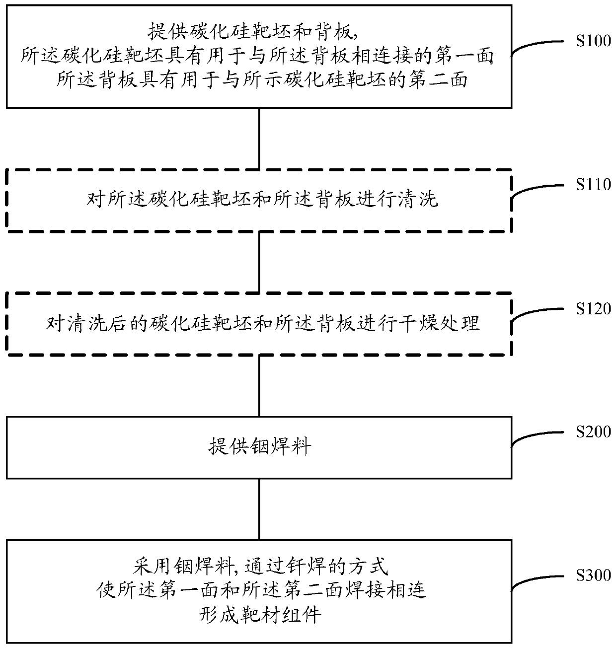
Figure 1 
Figure 2 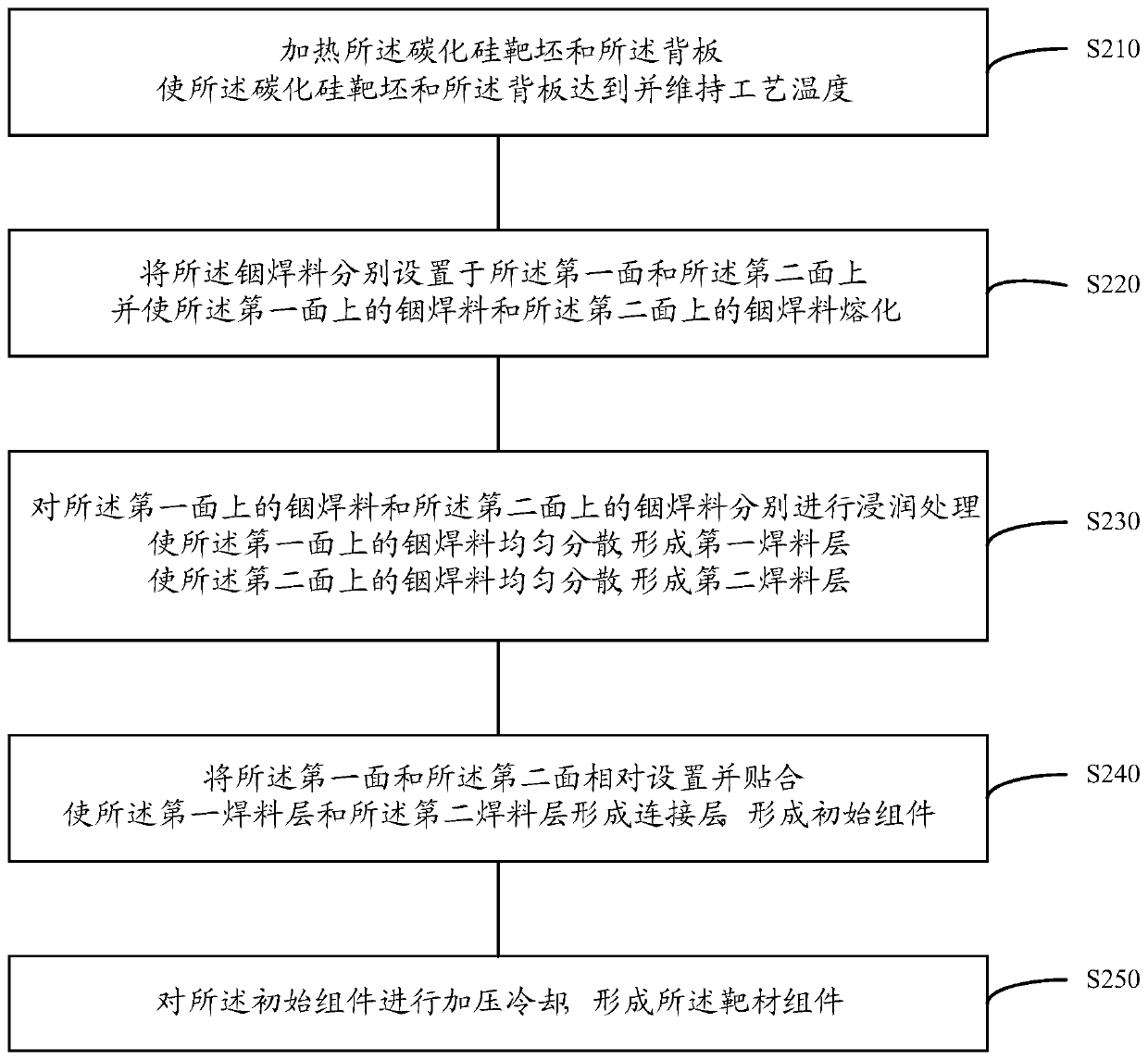
Figure 3
Abstract
Description
technical field
[0001] The invention relates to the field of target material manufacturing, in particular to a manufacturing method of a target material component. Background technique
[0002] Magnetron sputtering is a coating process that uses charged particles to bombard the target, causing the target atoms to overflow from the surface and evenly deposit on the substrate. Magnetron sputtering has the advantages of high sputtering rate, low substrate temperature, good bonding force between substrate and film, and excellent film uniformity. Magnetron sputtering technology has been widely used in the manufacturing process of electronic and information industries such as integrated circuits, information storage devices, liquid crystal displays, laser memories, and electronic control devices.
[0003] With the rapid development of the electronics industry, for example, in the manufacturing process of integrated circuits, the size of chip substrates continues to increase, whil...
Examples
Embodiment Construction
[0035] It can be seen from the background art that the silicon carbide target assembly in the prior art has the problem of low yield. Now combined with the structure of the silicon carbide target component to analyze the reasons for its low yield:
[0036] The silicon carbide target assembly is formed by welding the silicon carbide target blank and the back plate by using solder. In the prior art, the method of manufacturing silicon carbide target components usually uses tin solder to realize the welding of the two.
[0037] Silicon carbide material is relatively brittle, and it is prone to cracking during the manufacturing process of target components. Moreover, tin solder has high hardness after cooling and solidification, and it is difficult to play a buffering role between the silicon carbide target blank and the back plate. Therefore, in the prior art, tin solder is used to connect the silicon carbide target blank and the back plate by welding. SiC target blanks are pro...