
A high-power multi-channel waveguide microstrip synthesizer and its realization method
A high-power, combiner technology, used in waveguide-type devices, circuits, connecting devices, etc., can solve the problems of difficult to guarantee design size, reduced reliability, poor amplitude and phase consistency of multiple input powers, etc. Improve reliability and phase consistency
Patent Information
- Authority / Receiving Office
- CN · China
- Patent Type
- Patents(China)
- Current Assignee / Owner
- Publication Date
- 2021-08-06
Smart Images
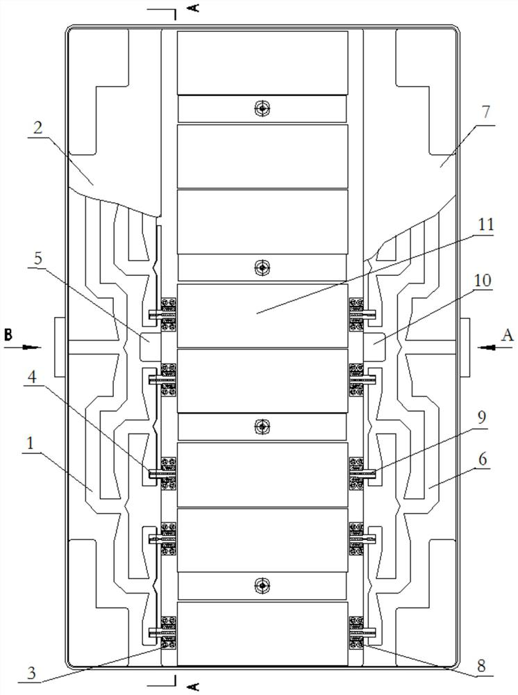
Figure 1 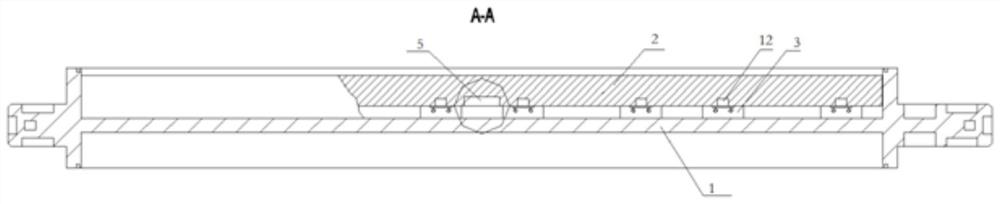
Figure 2 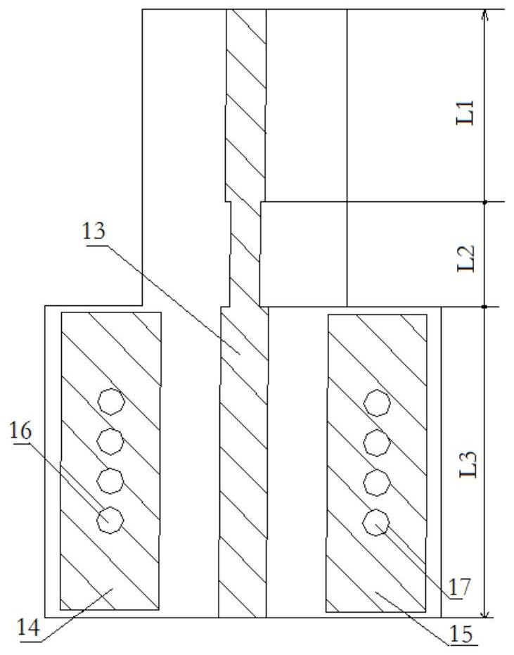
Figure 3
Abstract
Description
technical field
[0001] The invention belongs to the technical field of radar, communication system transmitter and microwave. Background technique
[0002] Solid-state transmitters are gradually replacing vacuum tube transmitters in modern radar and communication systems due to their characteristics of low operating voltage, high reliability, long life, good maintainability, failure weakening and fast switching capabilities. The solid-state power transmission component combines the output power of multiple power amplifier modules, and then combines the power generated by multiple solid-state power transmission components. The combined power is the output power of the high-power centralized solid-state transmitter. The working frequency of solid-state transmitters ranges from P, L, S bands to C, X bands, and even higher frequency bands such as Ku. Below the C-band, the solid-state power transmission components can use a stripline design power combining network to combine the...
Examples
Embodiment Construction
[0014] A kind of high-power multi-channel waveguide microstrip combiner that the present invention relates to and realization method, main realization process is as follows (referring to accompanying drawing):
[0015] (1) The spacing between the multi-channel input ends of the high-power multi-channel waveguide microstrip synthesizer is designed to be the width of the power amplifier module 11, and the waveguide power synthesis network is designed according to the width of the solid-state power transmitting component;
[0016] (2) Design the L1 part size of the waveguide microstrip conversion microstrip line 4 conductor strip 13 in the waveguide;
[0017] (3) According to the L1 part size of the microstrip line 4 conductor strip 13 in the waveguide, design the microstrip lining block 3 steps and the microstrip transition cavity 12;
[0018] (4) Weld the corresponding microstrip line 4 grounding boards of the L2 and L3 parts of the conductor strip 13 with the microstrip lining...