

Curved surface display panel
A curved surface display and panel technology, applied in nonlinear optics, instruments, optics, etc., can solve the problems of large relative movement, unevenness, and degradation of display quality between the light-shielding part and the pixel electrode, and achieve the effect of improving optical taste
Patent Information
- Authority / Receiving Office
- CN · China
- Patent Type
- Applications(China)
- Current Assignee / Owner
- Publication Date
- 2019-09-24
- Estimated Expiration
- Not applicable · inactive patent
Smart Images
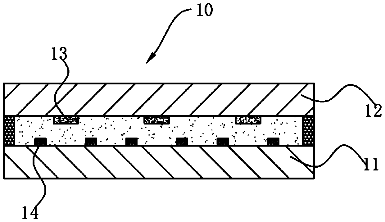
Figure 1 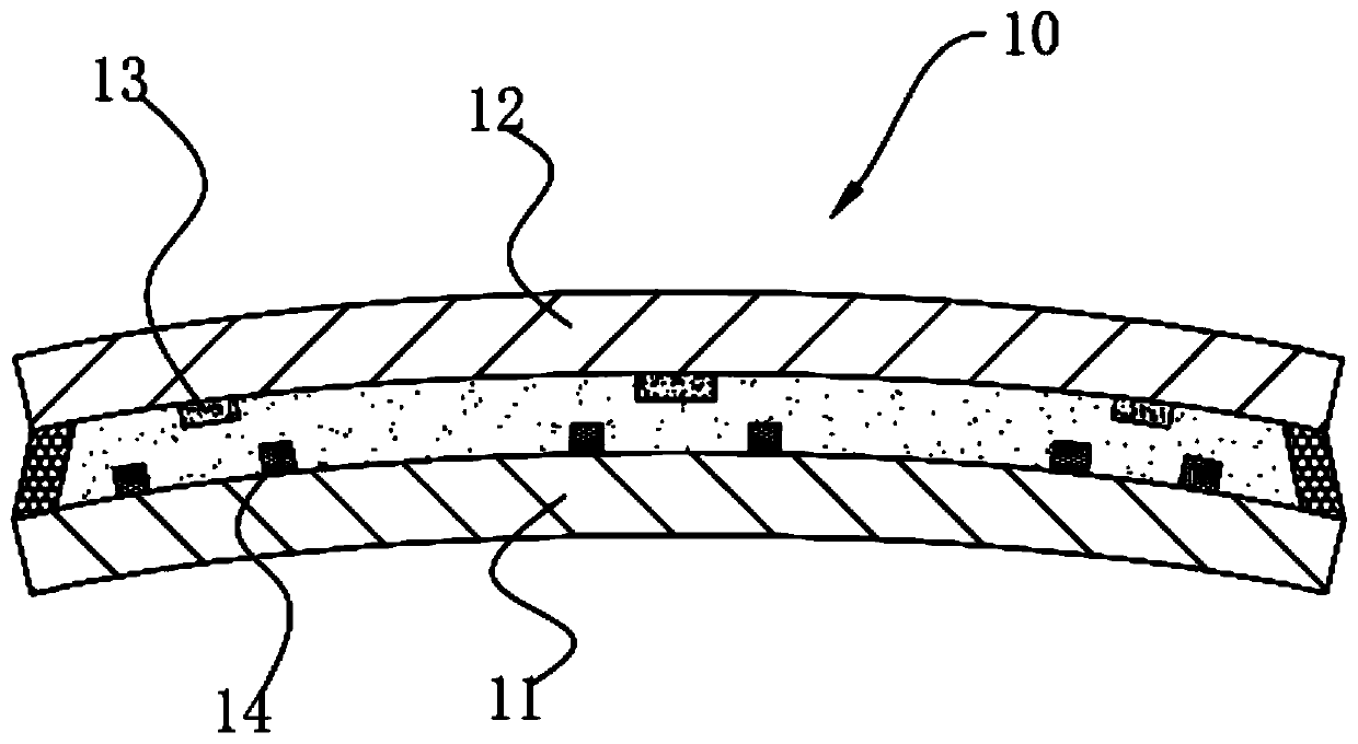
Figure 2 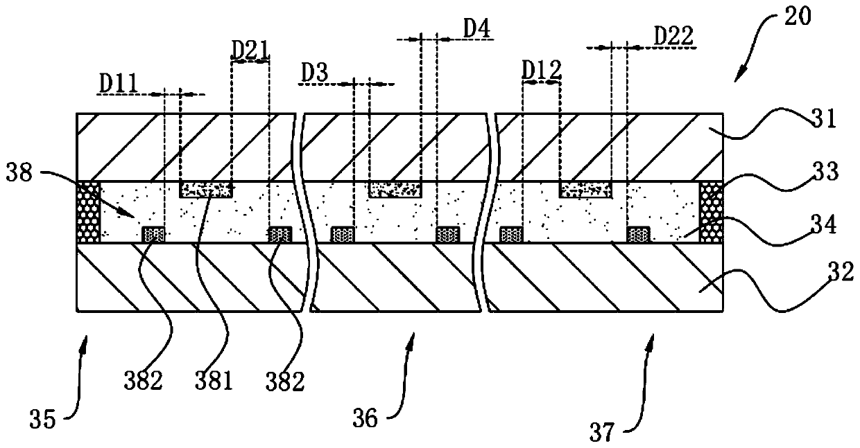
Figure 3
Abstract
Description
technical field
[0001] The invention relates to the field of display technology, in particular to a curved display panel. Background technique
[0002] The curved LCD panel is the core component of the curved LCD. Such as figure 1 As shown, the existing curved liquid crystal panel 10 generally includes a color filter (CF) substrate 11 and a thin film silicon transistor (TFT) substrate 12 oppositely arranged, and the pixel electrodes 13 arranged at intervals are arranged on the TFT substrate 12, and the CF A black matrix formed of a black color resist material is provided on the substrate 11. The black matrix includes a plurality of light-shielding parts 14 arranged at intervals. The positions of the light-shielding parts 14 and the pixel electrodes 13 are arranged alternately. , the distance between the light shielding portion 14 and the corresponding pixel electrode 13 is a set value.
[0003] However, if figure 2 As shown, when the curved liquid crystal panel 10 is in...
Examples
Embodiment 1
[0034] A curved display panel such as image 3 and Figure 4 As shown, the curved display panel 30 is formed by bending the flat display panel 20; the curved display panel 30 includes a curved color filter substrate 32, a curved surface array substrate 31, and The liquid crystal layer 34 on the 31 and the sealant 33; the sealant 33, the curved color filter substrate 32 and the curved array substrate 31 directly form an accommodating chamber for accommodating the liquid crystal layer 34.
[0035] Specifically, the side of the curved color filter substrate 32 away from the curved array substrate 31 is the light emitting surface of the curved display panel 30 , and the light emitting surface of the curved display panel 30 is a concave surface.
[0036] Specifically, a black matrix and a plurality of sub-pixels arranged at intervals are arranged between the curved surface array substrate 31 and the curved color filter substrate 32, and the black matrix includes light-shielding el...
Embodiment 2
[0062] A curved display panel such as Figure 7 and Figure 8 As shown, the difference from Embodiment 1 is that the display surface of the curved display panel 30 is convex.
[0063] Specifically, when the curved display panel 30 is in a flattened state, D21 is smaller than D11, and D12 is smaller than D22.
[0064] It should be noted that those skilled in the art know that when the light-emitting surface of the curved display panel 30 is convex, during the process of bending the flat display panel 20 into the curved display panel 30, the left end of the curved array substrate 31 moves relatively to the left, and the right end Relatively move to the right; when the curved display panel 30 is in a flattened state, D21 is set to be smaller than D11, and D12 is smaller than D22. When the flat display panel 20 is bent into a curved display panel 30, displacement compensation is used to make D21 equal to or D11 is approximately equal to D12, and D12 is equal to or approximately ...