
Silicon carbide MPS diode with high surge current
A technology of inrush current and silicon carbide, which is applied in the field of diodes, can solve problems such as diode failure and large PN junction conduction voltage, and achieve the effects of reducing on-resistance, reducing chip temperature, and improving anti-surge current capability
Patent Information
- Authority / Receiving Office
- CN · China
- Patent Type
- Applications(China)
- Current Assignee / Owner
- Publication Date
- 2022-04-01
Smart Images
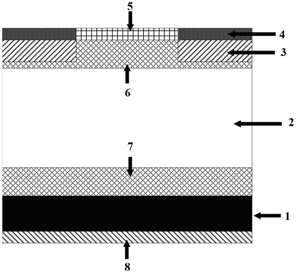
Figure 1 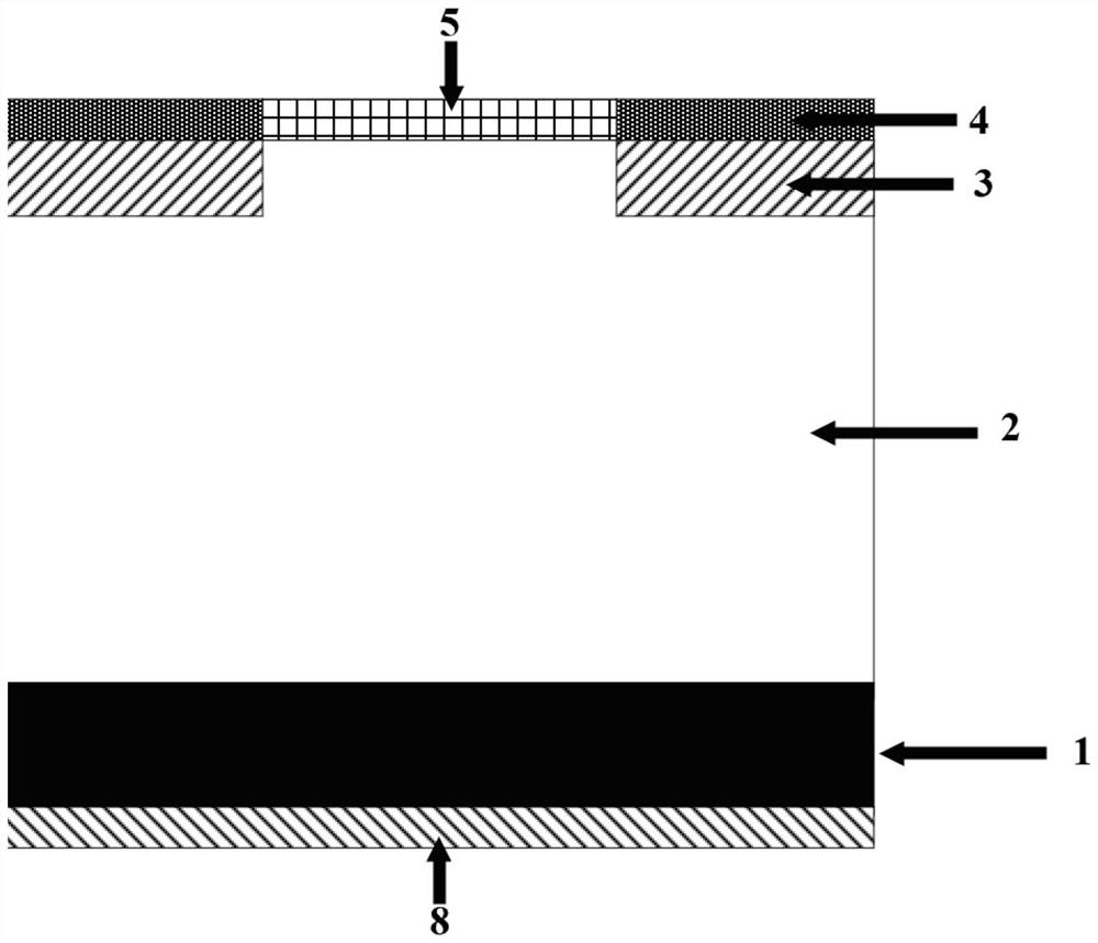
Figure 2 
Figure 3
Abstract
Description
technical field
[0001] The invention relates to the technical field of diodes. Background technique
[0002] Silicon carbide (SiC), a wide bandgap semiconductor material, is an ideal material for preparing high-voltage power electronic devices. Compared with Si materials, SiC materials have a higher breakdown electric field strength (4×10 6 V / cm), high carrier saturation drift velocity (2×10 7 cm / s), high thermal conductivity, and good thermal stability, so it is especially suitable for high-power, high-pressure, and high-temperature application scenarios. SiC Junction Barrier Schottky Diodes (JBS), as the earliest commercialized product in SiC power devices, now occupy the largest number of market shares. Through the potential barrier formed by the contact between SiC semiconductor and metal, the rectification effect of conducting in one direction and blocking in one direction is realized. The advantages of JBS diodes in power systems are the advantages of low on-resista...
Examples
Embodiment Construction
[0022] Referring to the accompanying drawings, through the description of the embodiments, the specific embodiments of the present invention include the shape, structure, mutual position and connection relationship of each part, the function and working principle of each part, and the manufacturing process of the various components involved. And the method of operation and use, etc., are described in further detail to help those skilled in the art have a more complete, accurate and in-depth understanding of the inventive concepts and technical solutions of the present invention.
[0023] Such as figure 1 As shown, it is a schematic diagram of the silicon carbide MPS diode layer structure with high surge current in the present invention, including ohmic contact electrode 4, silicon carbide N+ substrate 1, silicon carbide N- epitaxial layer 2, Schottky contact electrode 5, multiple P+ injection region 3, first bipolar transport layer 6, second bipolar transport layer 7, cathode ...