
Single-electron memory unit with nano metal oxide wire
A nano-metal, storage unit technology, applied in electrical components, nanotechnology, nanotechnology, etc., can solve the problems of complexity, high operating voltage, and unfavorable stabilization of single-electron memory performance, and achieve simple process and stable operation. Good results
Patent Information
- Authority / Receiving Office
- CN · China
- Patent Type
- Patents(China)
- Current Assignee / Owner
- Publication Date
- 2004-09-15
- Estimated Expiration
- Not applicable · inactive patent
Smart Images
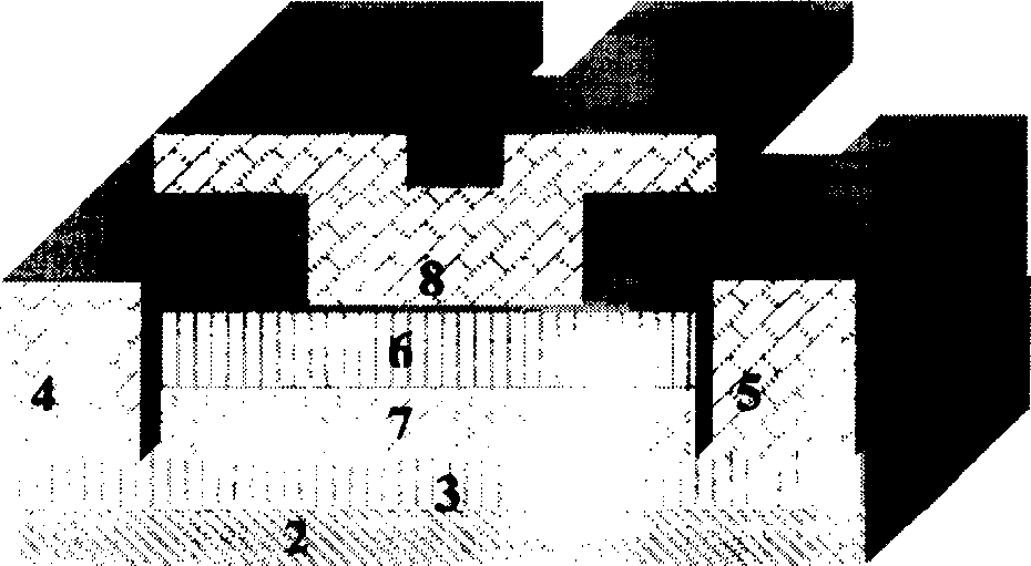
Figure 1 
Figure 2
Abstract
Description
Technical field:
[0001] The invention relates to a nanometer metal oxide wire single-electron storage unit, which is used in the technical field of nanometer electronics. Background technique:
[0002] Due to the limitation of the principle structure, the traditional silicon MOS memory cannot be single in T Bit (10 12 Bit) play a leading role in ultra-high-density integrated nano-memory. This is because this memory uses a MOS transistor T (often called a gate) controlled by a word line and a capacitor C that stores digital information (0 or 1). S (often called storage capacitance), one of the most important technical indicators of this memory is the charge transfer rate T of the unit Q , in order to ensure correct detection of stored information, T Q Bigger is better, and T Q The size depends on the storage capacitor C S Parallel capacitance C B Ratio, the larger the ratio, the better. C B Limited by the overall design, the minimum is 10 -12 F level. Therefore, onl...
Examples
Embodiment Construction
[0011] figure 1 It is a schematic diagram of a three-dimensional structure of an ultra-thin nanometer metal oxide wire TiOx single-electron storage unit according to an embodiment of the present invention.
[0012] Such as figure 1 As shown, the ultra-thin nanometer metal oxide line TiOx single-electron storage unit includes: silicon substrate 2, insulating layer 3 and insulating layer 6, source line 4; data line 5, active area 7 of memory unit, write line 8 . There is a layer of silicon dioxide insulating layer 3 on the silicon substrate 2, an ultra-thin titanium film is deposited on the insulating layer 3, and the active area 7 of the memory cell is locally oxidized, between the active area 7 and the write line 8 of the upper layer Au There is a layer of SiO 2 The insulating layer 6, the source line 4 of Au / Ti and the data line 5 of Au / Ti are located in the active area 7 and SiO 2 both sides of the insulating layer 6. Wherein, the length of the active region 7 is the di...