
Memory cell, memory device and manufacturing method of memory cell
A technology of memory cells and manufacturing methods, applied in static memory, digital memory information, electrical components, etc., can solve the problems of shortening the effective gate length, deterioration of transistor characteristics, etc. Effect
Patent Information
- Authority / Receiving Office
- CN · China
- Patent Type
- Patents(China)
- Current Assignee / Owner
- Publication Date
- 2011-01-26
- Estimated Expiration
- Not applicable · inactive patent
Smart Images
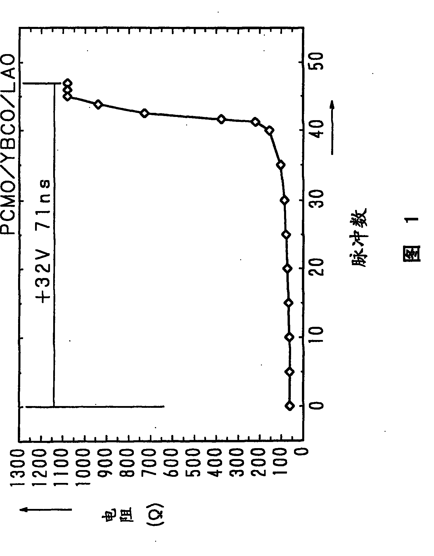
Figure 1 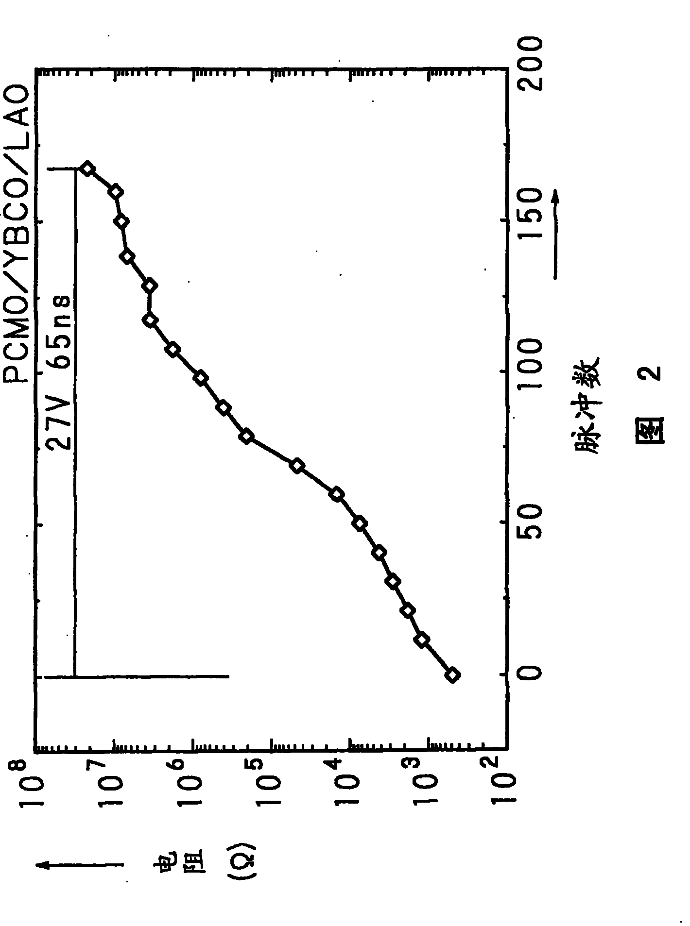
Figure 2 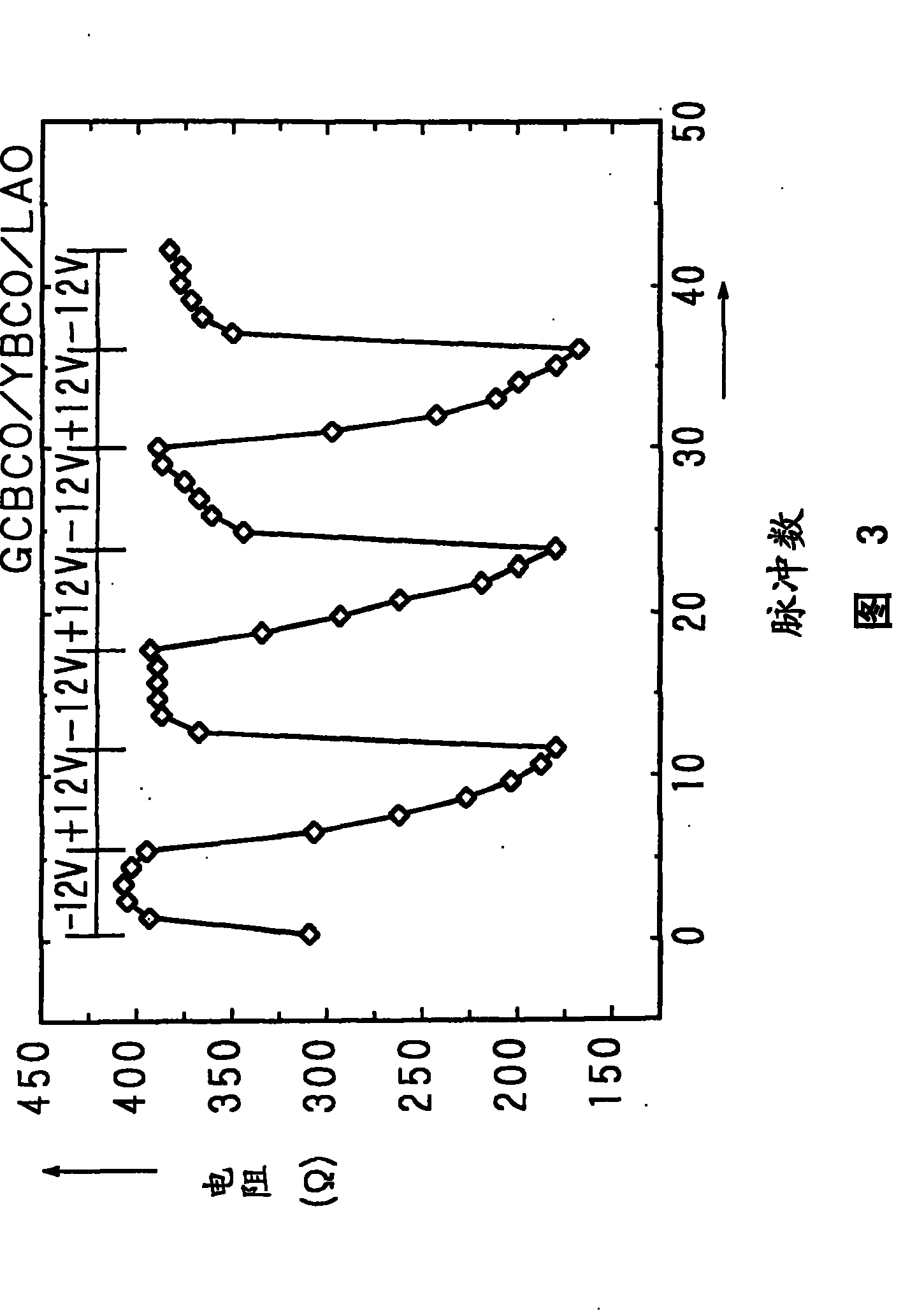
Figure 3
Abstract
Description
technical field
[0001] The present invention relates to a storage unit of 1D1R type (the unit cell is composed of a diode and an adjustable resistance element) composed of a series circuit of an adjustable resistance element and a Schottky diode, and relates to setting these storage units in a matrix. A memory device for a cell and a method for manufacturing the memory cell. Background technique
[0002] Many MRAMs (Magnetic Random Access Memory) currently being developed are formed by forming a ferromagnetic memory cell for storing information through residual magnetism of a ferromagnetic material of a giant magnetoresistive material. The change in resistance value generated by the difference between the magnetization directions is converted into a voltage. There are metal wires for writing in the ferromagnetic memory cell, and the magnetization direction of the ferromagnetic memory cell changes in the magnetic field generated when milliampere-level current flows through t...
Examples
Embodiment 1
[0095] 6 to 12 are diagrams illustrating manufacturing steps of Embodiment 1 of the memory cell manufacturing method according to the present invention. In each figure, a memory cell area (hereinafter referred to as memory area) in which memory cells are formed and an external circuit area (hereinafter referred to as external area) in which external circuits are formed are shown on the left and right sides, respectively. Each figure shows a cross-sectional structure of a memory cell (a series circuit of a Schottky diode and an adjustable resistance element) and an external circuit (N-channel MOSFET used in the external circuit shown in the example) in manufacturing steps. In addition, in each figure, oblique lines indicating cross-sections are omitted. Although MOSFETs are usually composed of P-channel MOSFETs and N-channel MOSFETs, only N-channel MOSFETs are shown here for simplicity.
[0096] FIG. 6 is a schematic diagram describing the formation of an element isolation reg...
Embodiment 2
[0109] 13 to 20 are schematic diagrams illustrating manufacturing steps of Embodiment 2 of the method of manufacturing a memory cell according to the present invention. In each figure, a memory cell area in which memory cells are formed (hereinafter referred to as memory area) and an external circuit area in which external circuits are formed (hereinafter referred to as external area) are shown on the left and right sides, respectively. Each figure shows a cross-sectional structure of a memory cell (a series circuit of a Schottky diode and an adjustable resistance element) and an external circuit (N-channel MOSFET used in the external circuit shown in the example) in manufacturing steps. In the memory area, an external circuit (part of the external circuit, etc.) may be provided at the lower portion of the memory cell, taking the external circuit as an example, a MOSFET is shown formed at the lower portion of the memory cell. In addition, in each figure, oblique lines indicati...