
Semiconductor device manufacturing method thereof
A manufacturing method and semiconductor technology, applied in semiconductor/solid-state device manufacturing, semiconductor devices, transistors, etc., can solve problems such as low cost and miniaturization limitations, increase in current value, and increase in the number of components, and achieve device miniaturization, The effect of reducing costs and reducing the number of parts
Patent Information
- Authority / Receiving Office
- CN · China
- Patent Type
- Applications(China)
- Current Assignee / Owner
- Publication Date
- 2005-10-05
- Estimated Expiration
- Not applicable · inactive patent
Smart Images
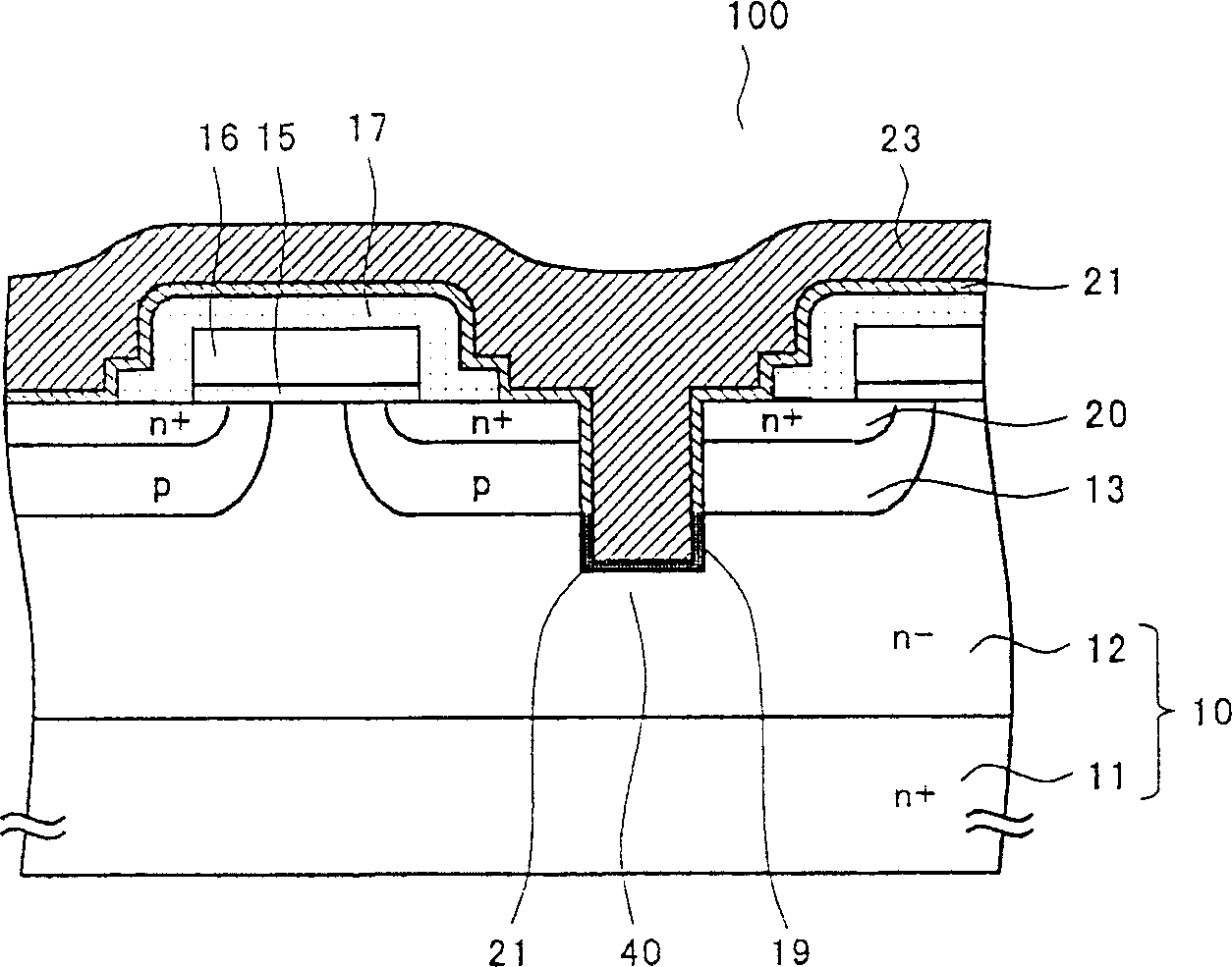
Figure 1 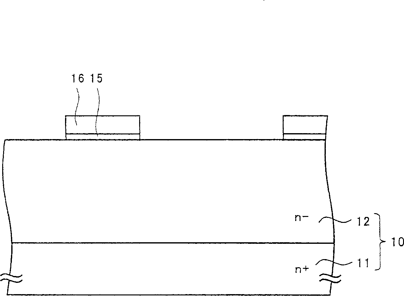
Figure 2 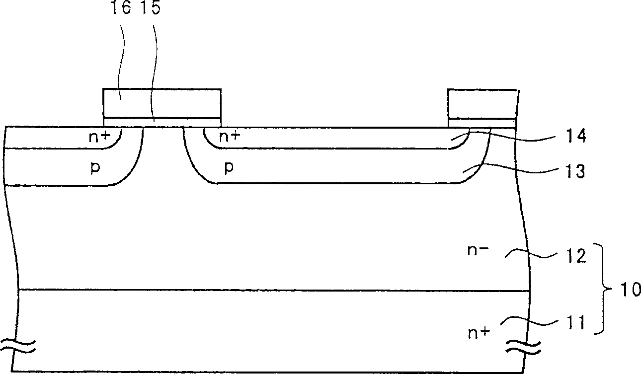
Figure 3
Abstract
Description
technical field
[0001] The present invention relates to a semiconductor device and a manufacturing method thereof, and more particularly to a semiconductor device incorporating a Schottky barrier diode in a MOSFET and a manufacturing method thereof. Background technique
[0002] Figure 14 Take n-channel type as an example to illustrate the structure of the existing MOSFET.
[0003] MOSFET 200 is composed of semiconductor substrate 130 , channel layer 133 , source region 134 , gate oxide film 135 , and gate electrode 136 .
[0004] The semiconductor substrate 130 is formed by laminating an n-type epitaxial layer 132 and the like on an n+ type silicon semiconductor substrate 131, and the n-type epitaxial layer 132 constitutes a drain region.
[0005] The channel layer 133 is formed on the surface of the semiconductor substrate in the field portion with a dose of 1.0×10 13 ~1.0×10 14 cm -2 Impurity diffusion region set by implanting p+ type ions.
[0006] The source regio...
Examples
Embodiment Construction
[0076] refer to Figure 1 to Figure 13 The embodiment of the present invention will be described in detail by taking an n-channel MOSFET as an example.
[0077] First, refer to Figure 1 to Figure 5 The first embodiment will be described. figure 1 is a cross-sectional view showing the MOSFET structure.
[0078] The MOSFET 100 is composed of a conductive semiconductor substrate 10 , a channel layer 13 , an insulating film 15 , a gate electrode 16 , a source region 20 , a groove 19 , a first metal layer 21 , and a second metal layer 23 .
[0079] A conductive type semiconductor substrate 10 is a substrate in which an n-type semiconductor layer 12 is stacked on an n+ type silicon semiconductor substrate 11 by epitaxial growth or the like, and the n-type semiconductor layer 12 constitutes a drain region.
[0080] The channel layer 13 is a p+ type impurity diffusion region provided on the surface of the n-type semiconductor layer 12 , and the source region 20 where phosphorus o...