
Channel MOS P-N junction Schottky diode structure and manufacturing method thereof
A technology of Schottky diode and channel structure, applied in semiconductor/solid-state device manufacturing, electrical components, circuits, etc., can solve the problems of low forward voltage drop value, consumption of conductive area, etc.
Patent Information
- Authority / Receiving Office
- CN · China
- Current Assignee / Owner
- Publication Date
- 2010-04-28
Smart Images
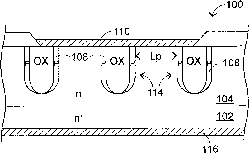
Figure 1 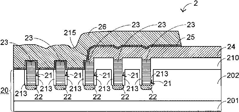
Figure 2 
Figure 3
Abstract
Description
technical field
[0001] The present invention relates to a kind of channel type Metal Oxide Semiconductor (MOS) P-N junction Schottky diode structure and its manufacturing method, especially relate to have lower leakage current, lower forward conduction voltage drop value (V F ), a higher reverse withstand voltage value, and a channel type metal oxide semiconductor P-N junction Schottky diode structure with low reverse recovery time characteristics. Background technique
[0002] Schottky diode is a unipolar element with electrons as carriers, and its characteristics are fast speed and forward conduction voltage drop value (V F ) is low, but the reverse bias leakage current is relatively large (related to the Schottky barrier value caused by the metal work function and semiconductor doping concentration). The P-N diode is a dual-carrier element that conducts a large amount of current. However, the forward conduction voltage drop of the component (V F ) is generally higher t...
Examples
Embodiment Construction
[0101] See figure 2 , which is a schematic diagram of a first preferred embodiment of a trenched metal-oxide-semiconductor P-N junction Schottky diode structure developed by the present invention to improve defects caused by known technical means. We can clearly see from the figure that the trench metal oxide semiconductor P-N junction Schottky diode structure 2 mainly includes a substrate 20, a channel structure 21, an ion implantation region 22, a polysilicon layer 23, an oxide Object layers 213, 210, 24 and metal layers 25, 26, wherein the substrate 20 is composed of a high doping concentration N-type silicon substrate (N+ silicon substrate) 201 and a low doping concentration N-type epitaxial layer (N- epitaxial layer) 202; the channel structure 21 is formed in the substrate 20 and the oxide layer 210, 213; the ion implantation region 22 is formed in the low doping concentration N-type epitaxial layer 202, and is formed in the channel The polysilicon layer 23 in the struc...