
SiC vertical double diffused metal-oxide-semiconductor (VDMOS) device and fabrication method thereof
A technology of silicon carbide and silicon carbide area, applied in semiconductor/solid-state device manufacturing, semiconductor devices, electrical components, etc., can solve problems such as rising system cost, low working speed, and increased volume
Patent Information
- Authority / Receiving Office
- CN · China
- Patent Type
- Applications(China)
- Current Assignee / Owner
- Publication Date
- 2017-10-13
Smart Images
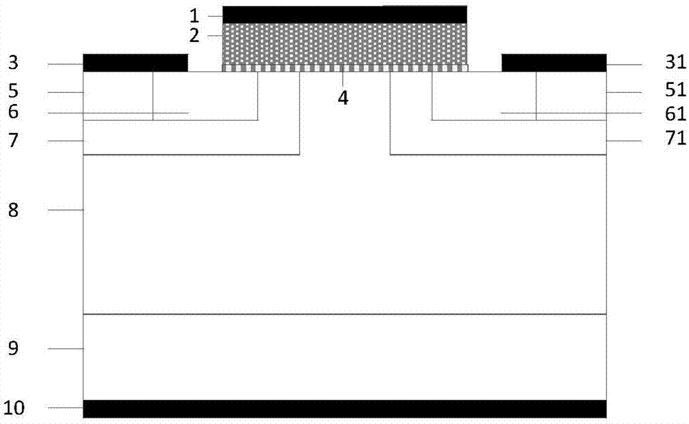
Figure 1 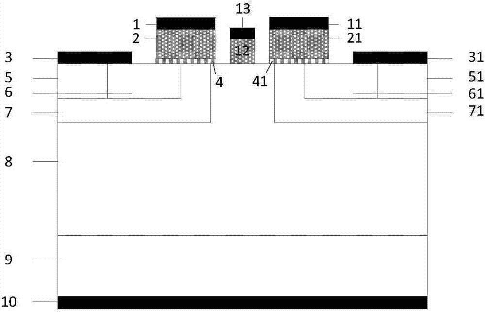
Figure 2 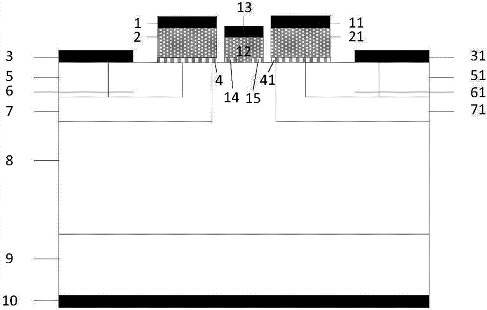
Figure 3
Abstract
Description
technical field
[0001] The invention belongs to the technical field of power semiconductors, and in particular relates to a silicon carbide VDMOS device and a manufacturing method thereof. Background technique
[0002] Since mankind entered the 21st century, energy issues have become increasingly prominent. Today, as the call for energy saving and emission reduction is getting louder and louder, the problem of electric energy conversion in household appliances, electric vehicles, industrial production, and locomotive traction is particularly important. Researchers in the field of power electronics can optimize and improve the power management system. It seems very important.
[0003] Power devices are at the heart of modern power systems. Since the performance of traditional silicon-based power devices is very close to the limit of silicon materials, it is difficult to greatly improve their performance. Therefore, some wide-bandgap semiconductor materials such as silicon ...
Examples
Embodiment 1
[0062] A kind of silicon carbide VDMOS device provided by the present invention, the cell structure of its basic structure is as follows figure 2 shown. It includes a metal drain electrode 10 arranged sequentially from bottom to top with a thickness of about 0.5-6 μm and a doping concentration of 1×10 18 cm -3 ~1×10 19 cm -3 , N with a thickness of 50-200 μm + The substrate 9 has a thickness of 15-18 μm and a doping concentration of about 1×10 15 cm -3 ~5×10 16 cm -3 N - Epitaxial layer 8; above the N- epitaxial layer 8 has a doping concentration of 1×10 17 ~7×10 17 cm -3 1. Implant the first Pbase region 7 with a depth of about 0.5-1 μm, and the other end of the upper layer has a second Pbase region 71 with the same parameters; the first Pbase region 7 has mutually independent doping concentrations of 1×10 19 ~1×10 20 cm -3 , implanting the first N with a depth of about 0.3-0.5 μm + The source region 6 and the doping concentration are about 3×10 19 ~1×10 20 ...
Embodiment 2
[0064] except P + Both sides below the polysilicon layer 12 also have N - The first dielectric layer 14 and the second dielectric layer 15 in direct contact with the epitaxial layer 8 are the same as the first embodiment in the rest of the structure of this embodiment.
[0065] In diode application, the first dielectric layer 14 and the second dielectric layer 15 are at P + The electron accumulation layer formed under the polysilicon layer 12 can further reduce the drift region resistance of the device, thereby reducing the forward conduction voltage drop of the device.
Embodiment 3
[0067] divide by N - In the epitaxial layer 8 and under the first Pbase region 7, there is also a first P-type silicon carbide region 16 forming a super junction or semi-super junction structure, and the N - In the epitaxial layer 8 and below the first Pbase region 7 there is also a second P-type silicon carbide region 161 forming a superjunction or semi-superjunction structure, and the rest of the structure of this embodiment is the same as that of Embodiment 1.
[0068] The formation of a superjunction or semi-superjunction structure can further reduce the drift region resistance of the device in diode applications and MOS applications, thereby reducing the forward conduction voltage drop of the device.
[0069] and figure 1 Compared with the cell structure of the traditional silicon carbide VDMOS device shown, the present invention deposits a polysilicon layer on the surface of the JFET region of the silicon carbide VDMOS device to form a Si / SiC heterojunction. Applicatio...