
Making process of fast recovery chip
A manufacturing process and chip technology, which is applied to the manufacturing process of fast recovery chips, can solve the problems of high failure rate and low reliability, and achieve the effects of low failure rate, high reliability and improved functional characteristics.
Patent Information
- Authority / Receiving Office
- CN · China
- Patent Type
- Applications(China)
- Current Assignee / Owner
- Publication Date
- 2016-09-28
Smart Images
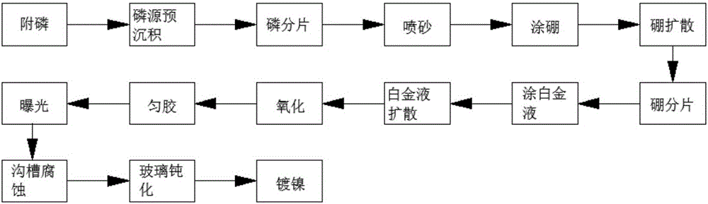
Figure 1 
Figure 2
Abstract
Description
technical field
[0001] The invention relates to the technical field of semiconductor devices, in particular to a manufacturing process of a fast recovery chip. Background technique
[0002] With the vigorous development of the semiconductor market, customers' demands for our products are also becoming more diversified and require higher reliability. In the current market, among the customers who mainly manufacture electronic circuits such as switching power supplies, modulators, and frequency converters, there is a great demand for fast recovery products, and the requirements for the characteristics of the products are also extremely strict. Therefore, in order to meet customers' demand for high-end products, fast recovery products are different from conventional products in that they have a low reverse recovery time, which requires doping during the grain production process, but in order to ensure that the grain itself has a relatively high High reliability and glass passi...
Examples
Embodiment 1
[0037] Such as figure 1 A fast recovery type chip fabrication process shown includes the following steps:
[0038] (1) Phosphorous attachment: first clean the silicon wafers, then sandwich the paper-like phosphorus source with a concentration of not less than 70% between adjacent silicon wafers, and place them on the quartz boat in turn; the silicon wafer cleaning steps are: First put the silicon wafer into the HF solution and soak for 2 minutes, wherein the ratio of the HF solution is HF:H2O=1000ml:8500ml, the temperature is 35°C, and then use the Harmo solution and hot pure water for ultrasonic vibration, the Harmo solution ratio is Harmo powder: H2O=200g: 18000ml, temperature: 85°C, time 20min, finally flushing, shaking with running water, flushing, drying, silicon wafers are cleaned;
[0039] (2) Phosphorus source pre-deposition: send the quartz boat equipped with silicon wafers into a diffusion furnace with a temperature of 600°C to decompose the phosphorus source for 2 ...
Embodiment 2
[0055] Such as figure 1 A fast recovery type chip fabrication process shown includes the following steps:
[0056] (1) Phosphorous attachment: first clean the silicon wafers, then sandwich the paper-like phosphorus source with a concentration of not less than 70% between adjacent silicon wafers, and place them on the quartz boat in turn; the silicon wafer cleaning steps are: First put the silicon chip into the HF solution and soak for 1min, wherein the ratio of the HF solution is HF:H2O=1000ml:8500ml, the temperature is 25°C, and then use the Harmo solution and hot pure water for ultrasonic vibration, the Harmo solution ratio is Harmo powder: H2O=200g: 18000ml, temperature: 75°C, time 10min, finally flushing, shaking with running water, flushing, drying, silicon wafers are cleaned;
[0057] (2) Phosphorus source pre-deposition: send the quartz boat equipped with silicon wafers into a diffusion furnace with a temperature of 550°C to decompose the phosphorus source for 1 hour, ...