
Wide dynamic range image sensor pixel cell
Patent Information
- Authority / Receiving Office
- US · United States
- Current Assignee / Owner
- Publication Date
- 2019-08-27
Smart Images
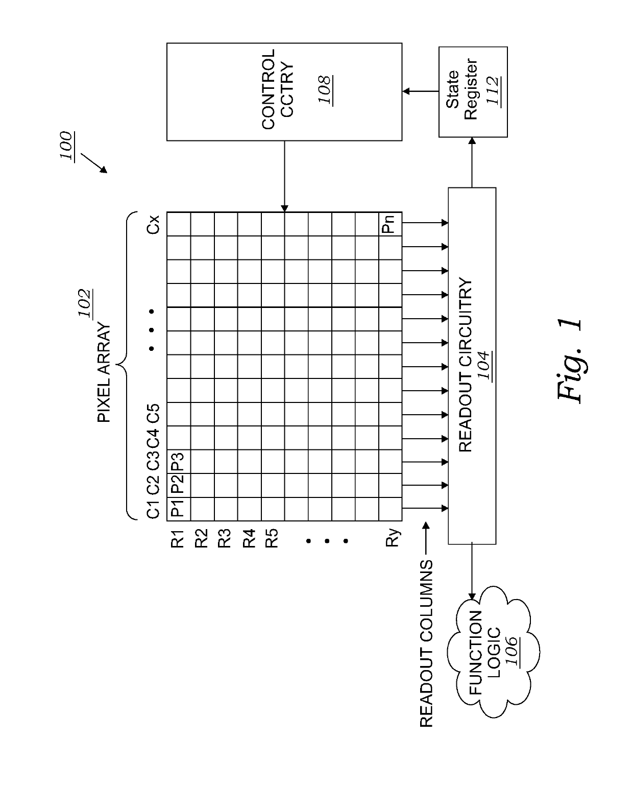
Figure 1 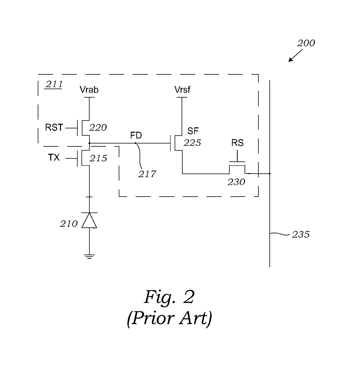
Figure 2 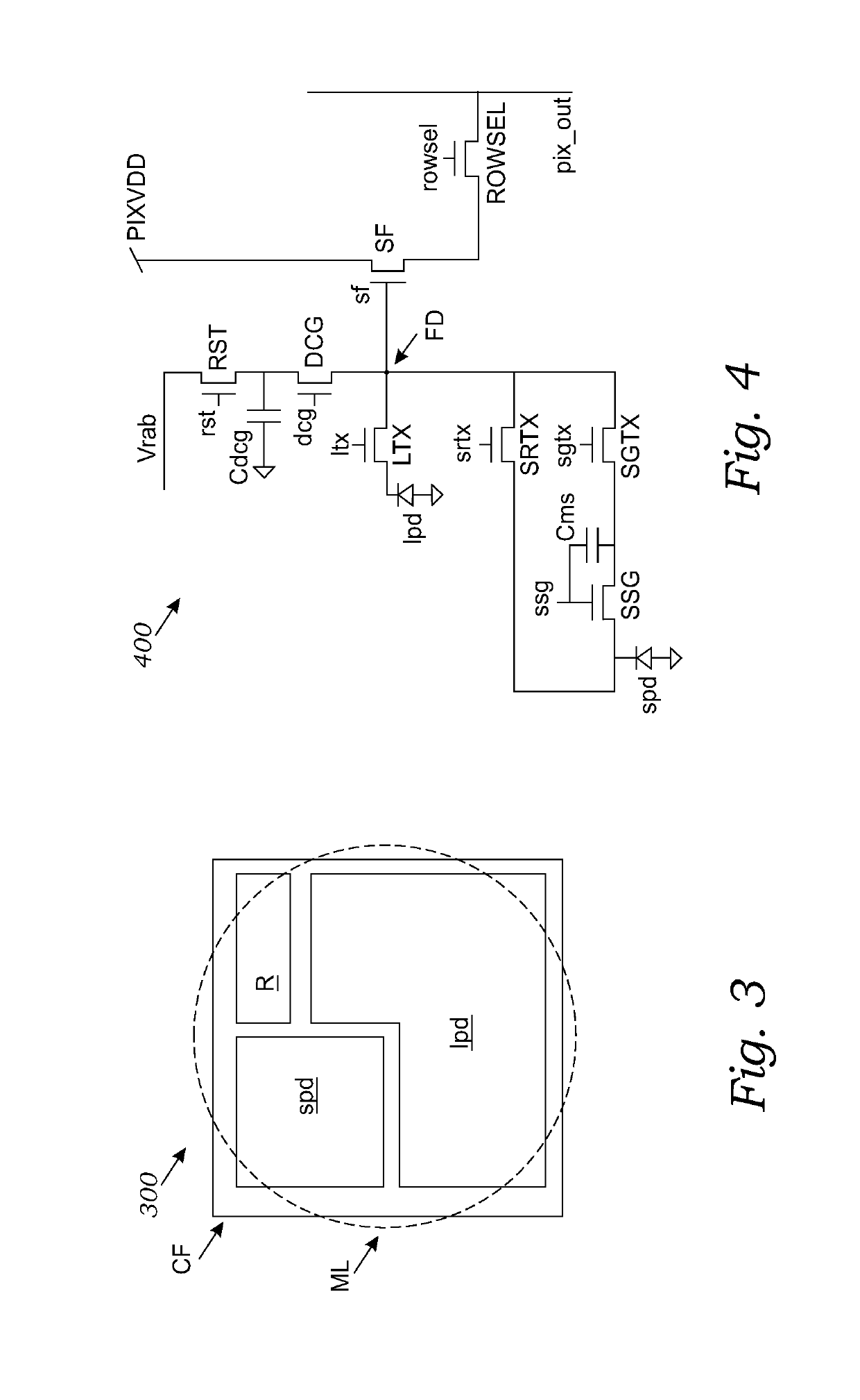
Figure 3
Abstract
Description
BACKGROUND OF THE INVENTIONField of the Invention
[0001] This invention relates generally to image sensors, and more particularly to CMOS image sensors. The present invention provides a pixel cell design and method for obtaining wide dynamic range images. An image sensor comprising the invented pixel design and method may be incorporated within a digital camera.Description of Related Art
[0002] An image capture device includes an image sensor and an imaging lens. The imaging lens focuses light onto the image sensor to form an image, and the image sensor converts the light into electrical signals. The electric signals are output from the image capture device to other components of a host electronic system. The image capture device and the other components of a host electronic system form an imaging system. Image sensors have become ubiquitous and may be found in a variety of electronic systems, for example a mobile device, a digital camera, a medical device, or a computer.
[0003] A typical...
Examples
first embodiment
[0039]In summary, as a result of the described circuit diagram of FIG. 4 and the described control signal timing diagram of the invention four separate signals and their respective reference levels are generated and readout for each pixel cell leading to a widening of the dynamic range of the resultant signal representing the illumination incident upon the dual photodiode pixel. An advantage of the invented pixel cell is that the dual conversion gain components are shared by the large and small photodiodes rather than constrained to have separate dual conversion gain components assigned to each photodiode. The read out methods illustrated in FIG. 5 would be more commonly be used in a row by row rolling shutter readout method for both the large and small photodiodes but the presence of storage elements Cms and SGTX it is to be understood that in another embodiment of the invention the small photodiode may be exposed and read out in a global shutter mode while the large photodiode is ...
second embodiment
[0041]FIG. 6 is an electrical schematic diagram of a pixel cell in accordance with the invention. FIG. 6 illustrates pixel cell 600 comprising the same signal dynamic range enhancing features shown in FIG. 4 but with an alternative connection scheme. The pixel cell electrical schematic illustrated in FIG. 6 is the same as the one shown in FIG. 4 with the exception that transistor SRTX connects small photodiode spd to node D, the node between dynamic enhancement capacitor Cdcg and capacitor control transistor DCG, rather than at the node between transistor DCG and floating drain FD. A control timing diagram similar to FIG. 5 can be used to read out imaging signals providing enhanced dynamic range.
[0042]Further embodiments of the invention may be realized by the choice of fabrication method for capacitors Cdcg and Cms. These capacitors may be fabricated as metal-insulator-metal (MIM) capacitors, metal-oxide-metal (MOM) capacitors or metal-oxide-silicon (MOS) capacitors. There are also...