
Dielectric waveguide filter
a filter and waveguide technology, applied in waveguides, resonators, electrical equipment, etc., can solve the problems of increasing the insertion loss in the pass band, and achieve the effects of steep attenuation characteristics, reduced or prevented, and steep attenuation characteristics
Patent Information
- Authority / Receiving Office
- US · United States
- Patent Type
- Patents(United States)
- Current Assignee / Owner
- Publication Date
- 2022-06-14
Smart Images
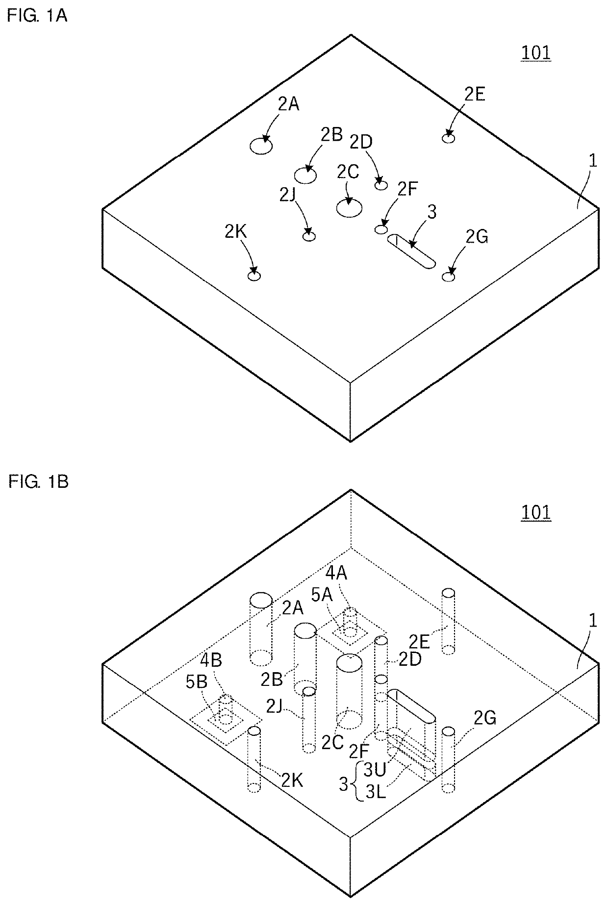
Figure 1 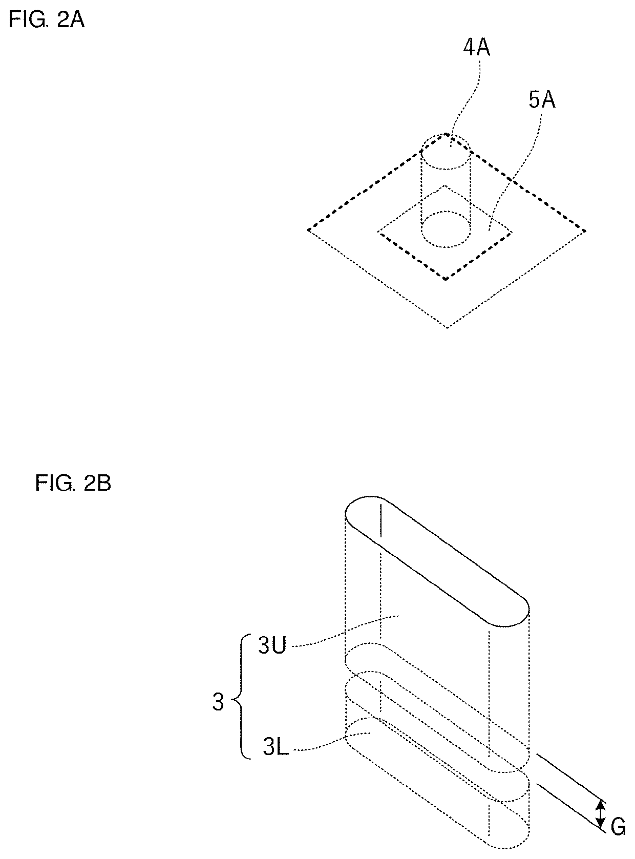
Figure 2 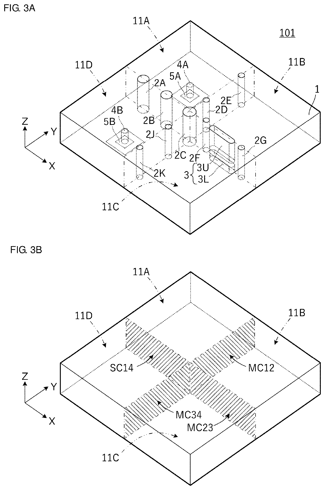
Figure 3
Abstract
Description
CROSS REFERENCE TO RELATED APPLICATIONS
[0001] This application claims the benefit of priority to Japanese Patent Application No. 2018-125911 filed on Jul. 2, 2018 and is a Continuation Application of PCT Application No. PCT / JP2019 / 020291 filed on May 22, 2019. The entire contents of each application are hereby incorporated herein by reference.BACKGROUND OF THE INVENTION1. Field of the Invention
[0002] The present invention relates to a dielectric waveguide filter that includes a plurality of dielectric waveguide resonators.2. Description of the Related Art
[0003] International Publication No. 2018 / 012294, for example, discloses a dielectric waveguide filter that includes a plurality of dielectric waveguide resonators. In the dielectric waveguide filter described in International Publication No. 2018 / 012294, a coupling portion is formed between resonators so as to couple adjacent dielectric waveguide resonators.
[0004] In a dielectric waveguide filter, in which a plurality of dielectric wav...
Examples
first preferred embodiment
[0032]FIG. 1A is an external perspective view of a dielectric waveguide filter 101 according to a first preferred embodiment of the present invention and FIG. 1B is a transparent perspective view illustrating an internal structure of the dielectric waveguide filter 101. FIG. 2A is an enlarged perspective view illustrating structures of an input / output post and an input / output pad and FIG. 2B is an enlarged perspective view illustrating structures of non-penetrating posts 3U and 3L. Further, FIG. 3A is a perspective view illustrating four dielectric waveguide resonator portions included in the dielectric waveguide filter 101 and FIG. 3B is a perspective view illustrating a main coupling portion and a sub coupling portion included in the dielectric waveguide filter 101.
[0033]The dielectric waveguide filter 101 is structured in a dielectric block 1 having a rectangular or substantially rectangular parallelepiped shape. The dielectric block 1 is formed by processing dielectric ceramic, ...
second preferred embodiment
[0057]A second preferred embodiment of the present invention describes a dielectric waveguide filter in which the number of stages of resonators is different from that of the first preferred embodiment.
[0058]FIG. 10A is an external perspective view of a dielectric waveguide filter 102 according to the second preferred embodiment and FIG. 10B is a transparent perspective view illustrating an internal structure of the dielectric waveguide filter 102.
[0059]This dielectric waveguide filter 102 is structured in a dielectric block 1 having a rectangular or substantially rectangular parallelepiped shape. Input / output pads 5A and 5B are provided on the bottom surface of the dielectric block 1. The dielectric block 1 includes input / output posts 4A and 4B respectively protruding from the input / output pads 5A and 5B to the inside of the dielectric block 1. Further, the dielectric block 1 includes penetrating posts 2A, 2B, 2C, 2D, 2E, and 2F penetrating from the upper surface to the lower surfa...
third preferred embodiment
[0071]A third preferred embodiment of the present invention describes some examples of a dielectric waveguide filter in which structures of inductive coupling portions and capacitive coupling portions are different from those of the dielectric waveguide filter described in the second preferred embodiment.
[0072]FIG. 13A is an external perspective view of a dielectric waveguide filter 103A according to the third preferred embodiment and FIG. 13B is a transparent perspective view illustrating an internal structure of the dielectric waveguide filter 103A.
[0073]The dielectric waveguide filter 103A is structured in a dielectric block 1 having a rectangular or substantially rectangular parallelepiped shape. The dielectric block 1 includes penetrating posts 2AD, 2BE, and 2CF penetrating from the upper surface to the lower surface of the dielectric block 1. The penetrating post 2AD is provided by connecting and integrating the penetrating post 2A and the penetrating post 2D included in the d...