
Dielectric waveguide filter
A waveguide and dielectric technology, applied in the field of dielectric waveguide filters, can solve the problems of large size and increase of passband insertion loss, etc.
Patent Information
- Authority / Receiving Office
- CN · China
- Patent Type
- Applications(China)
- Current Assignee / Owner
- Publication Date
- 2022-07-12
Smart Images
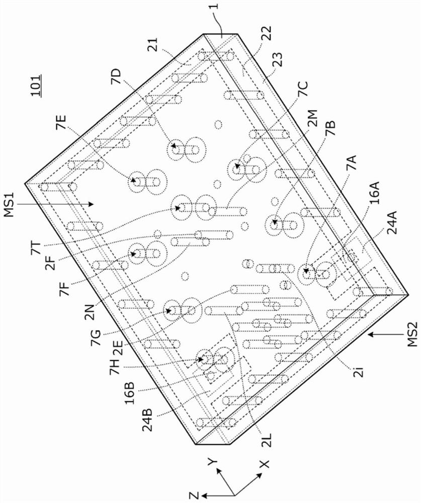
Figure 1 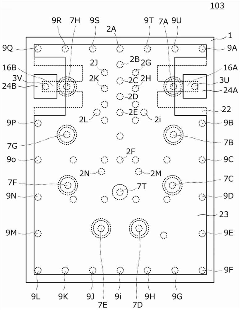
Figure 2 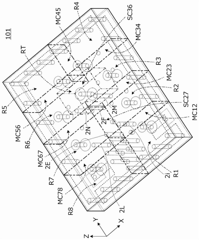
Figure 3
Abstract
Description
technical field
[0001] The present invention relates to a dielectric waveguide filter including a plurality of dielectric waveguide resonators. Background technique
[0002] For example, Patent Document 1 discloses a dielectric waveguide filter including a plurality of dielectric waveguide resonators. The dielectric waveguide filter described in Patent Document 1 includes a coupling portion between the resonators so that adjacent dielectric waveguide resonators are coupled to each other.
[0003] In the dielectric waveguide filter shown in Patent Document 1 in which a plurality of dielectric waveguide resonators are arranged and adjacent dielectric waveguide resonators are coupled to each other, the adjacent dielectric waveguides along the main path of signal transmission resonate The resonators are coupled to each other and can constitute a secondary path coupled across a plurality of dielectric waveguide resonators in sequence on the primary path.
[0004] Patent Documen...
Examples
no. 1 approach 》
[0045] figure 1 It is a perspective view showing the internal structure of the dielectric waveguide filter 101 according to the first embodiment. figure 2 This is a bottom view of the dielectric waveguide filter 101 . in addition, image 3 It is a perspective view showing nine dielectric waveguide resonator parts, a main coupling part and a sub coupling part between the dielectric waveguide resonators, which are included in the dielectric waveguide filter 101 .
[0046]The dielectric waveguide filter 101 includes the dielectric plate 1 . The dielectric plate 1 is, for example, a member obtained by processing a dielectric ceramic, crystal, resin, or the like into a rectangular parallelepiped shape. The dielectric plate 1 has a first main surface MS1 and a second main surface MS2 facing each other, and four side surfaces SS connecting the outer edge of the first main surface MS1 and the outer edge of the second main surface MS2. In this example, the dimensions of the dielec...
no. 2 approach 》
[0090] In the second embodiment, a dielectric waveguide filter in which the number of stages of resonators is different from the dielectric waveguide filter shown in the first embodiment is shown.
[0091] Figure 10 of (A), Figure 10 (B) is a diagram showing a coupling structure of a plurality of resonators constituting the dielectric waveguide filter 102 of the second embodiment. exist Figure 10 of (A), Figure 10 In (B), resonator R1 is the first-stage (primary) resonator, resonator R2 is the second-stage resonator, resonator R3 is the third-stage resonator, and resonator R4 is the fourth-stage resonator. Resonator R5 is the fifth stage resonator and resonator R6 is the sixth stage (final stage) resonator. exist Figure 10 of (A), Figure 10 In (B) of , the path shown by the double-dashed line is the main coupling part, and the broken line is the sub coupling part. In addition, in Figure 10 of (A), Figure 10 In (B) of , "L" indicates inductive coupling and "C" ...
no. 3 approach 》
[0095] In the third embodiment, an example of a mobile phone base station to which a dielectric waveguide filter is applied is shown.
[0096] Figure 11 is a block diagram of a mobile phone base station. The circuit of the mobile phone base station includes: FPGA 121, DA converter 122, bandpass filters 123, 126, 131, single mixer 125, local oscillator 124, attenuator 127, amplifier 128, power amplifier 129, detection device 130 and antenna 132.
[0097] The above-mentioned FPGA 121 generates a modulated digital signal. The DA converter 122 converts the modulated digital signal into an analog signal. The bandpass filter 123 passes signals in the baseband frequency band and removes signals in other frequency bands. The single mixer 125 mixes and upconverts the output signal of the bandpass filter 123 and the oscillation signal of the local oscillator 124 . Band pass filter 126 removes unnecessary frequency bands resulting from up-conversion. The attenuator 127 adjusts the i...