
Photodiode with ultra-shallow junction for high quantum efficiency CMOS image sensor and method of formation
a photodiode and ultra-shallow junction technology, applied in the field of semiconductor devices, can solve the problems of complex design of photodiodes for the blue spectrum, surface defects, and minority carriers in blue pixel sensor cells are substantially more likely to be lost in recombination, so as to achieve the effect of maximizing blue light absorption and improving the blue response in the photosensor
Patent Information
- Authority / Receiving Office
- US · United States
- Patent Type
- Applications(United States)
- Current Assignee / Owner
- Publication Date
- 2005-08-04
Smart Images
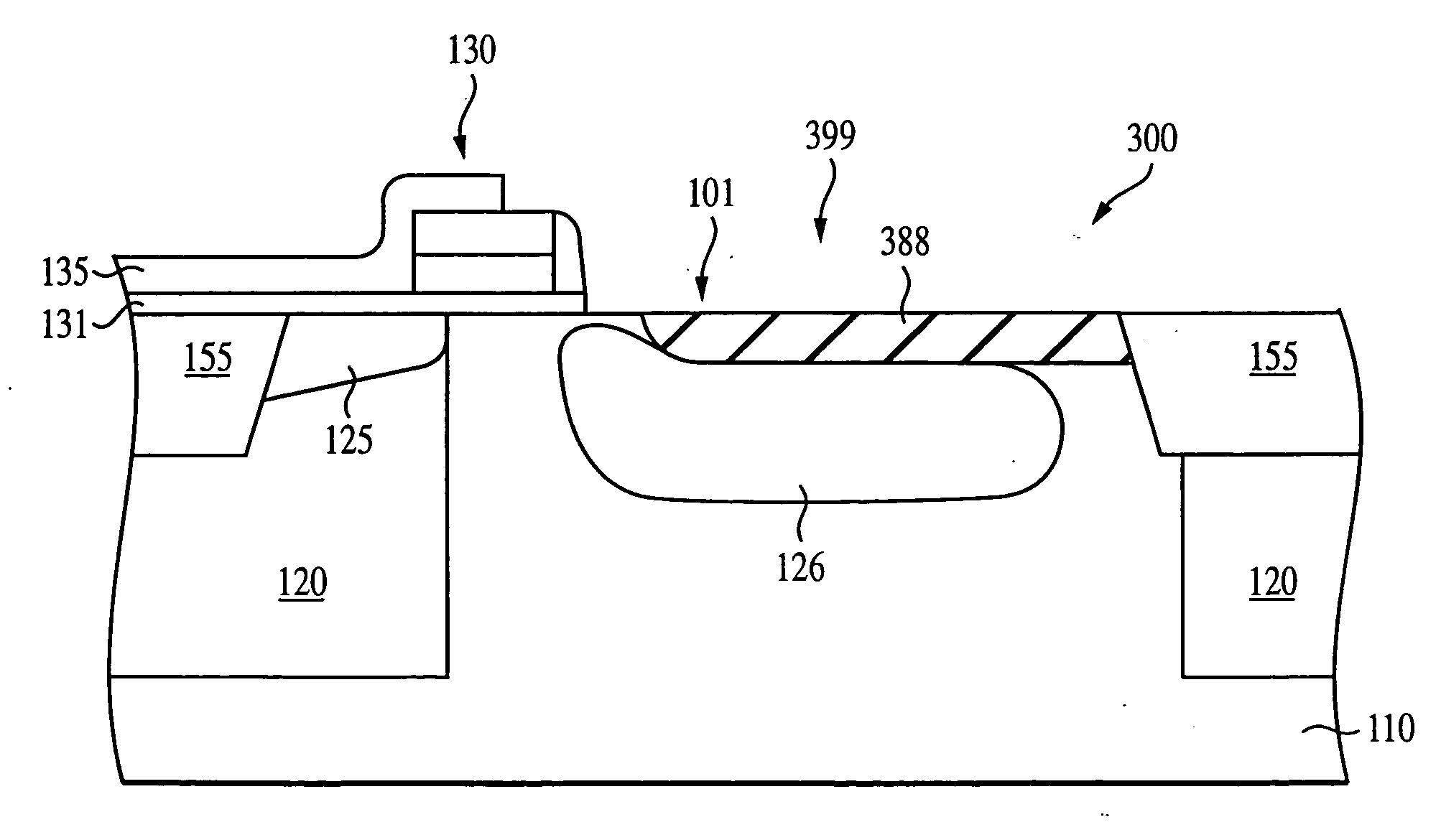
Figure 1 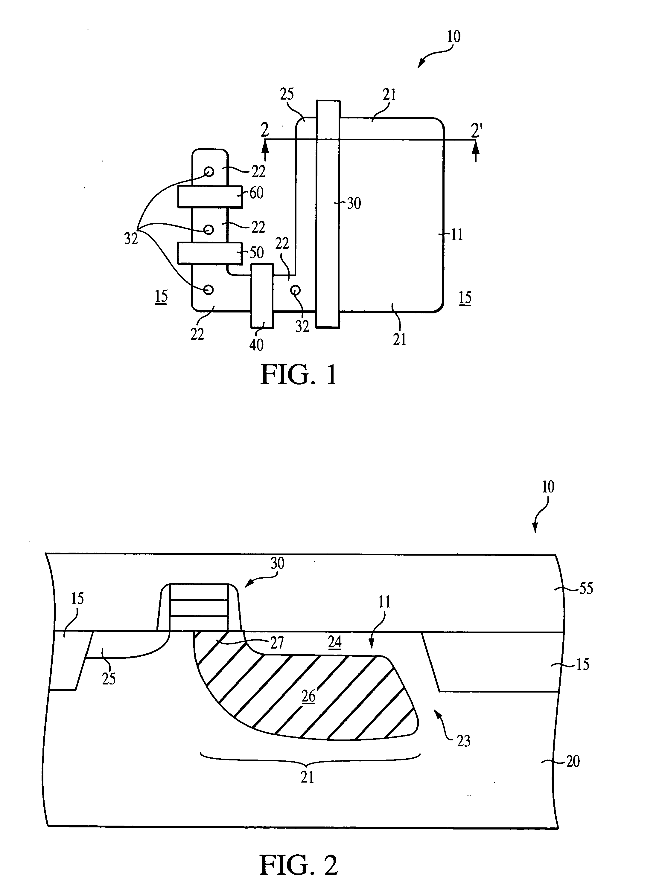
Figure 2 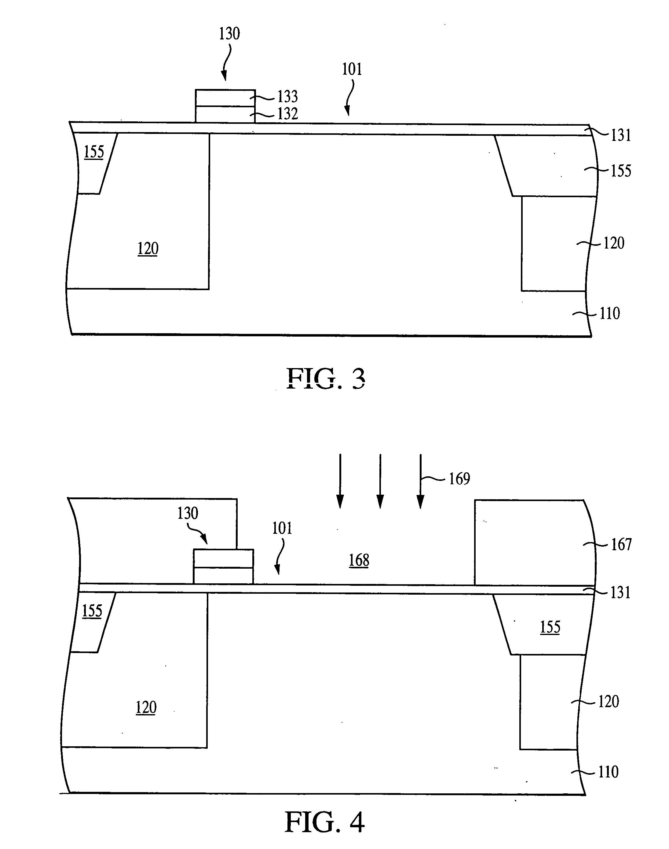
Figure 3
Abstract
Description
CROSS REFERENCE TO OTHER APPLICATON
[0001] This application claims priority to U.S. Provisional Patent Application No. 60 / 478,359 filed on Jun. 16, 2003 which is hereby incorporated by reference in its entirety.FIELD OF THE INVENTION
[0002] The present invention relates to the field of semiconductor devices and, in particular, to improved photodiodes for high quantum efficiency. BACKGROUND OF THE INVENTION
[0003] The semiconductor industry currently uses different types of semiconductor-based imagers, such as charge coupled devices (CCDs), photodiode arrays, charge injection devices and hybrid focal plane arrays, among others.
[0004] Because of the inherent limitations and expense of CCD technology, CMOS imagers have been increasingly used as low cost imaging devices. A CMOS imager circuit includes a focal plane array of pixel cells, each one of the cells including either a photodiode, a photogate or a photoconductor overlying a doped region of a substrate for accumulating photo-gen...
Examples
Embodiment Construction
[0036] In the following detailed description, reference is made to the accompanying drawings which form a part hereof, and in which is shown by way of illustration specific embodiments in which the invention may be practiced. These embodiments are described in sufficient detail to enable those skilled in the art to practice the invention, and it is to be understood that other embodiments may be utilized, and that structural, logical and electrical changes may be made without departing from the spirit and scope of the present invention.
[0037] The terms “wafer” and “substrate” are to be understood as a semiconductor-based material including silicon, silicon-on-insulator (SOI) or silicon-on-sapphire (SOS) technology, doped and undoped semiconductors, epitaxial layers of silicon supported by a base semiconductor foundation, and other semiconductor structures. Furthermore, when reference is made to a “wafer” or “substrate” in the following description, previous process steps may have be...