
Method and apparatus for measuring three-dimensional shape of specimen by using SEM
a three-dimensional shape and specimen technology, applied in the field of methods and apparatus for measuring or estimating the three-dimensional profile of specimens, can solve the problems of difficult to accurately estimate the height information on a flat portion or a nearly vertical portion, and the pre-process for manufacturing these devices is becoming increasingly difficult to control, so as to achieve accurate measurement of the three-dimensional profile
Patent Information
- Authority / Receiving Office
- US · United States
- Current Assignee / Owner
- Publication Date
- 2005-12-29
Smart Images
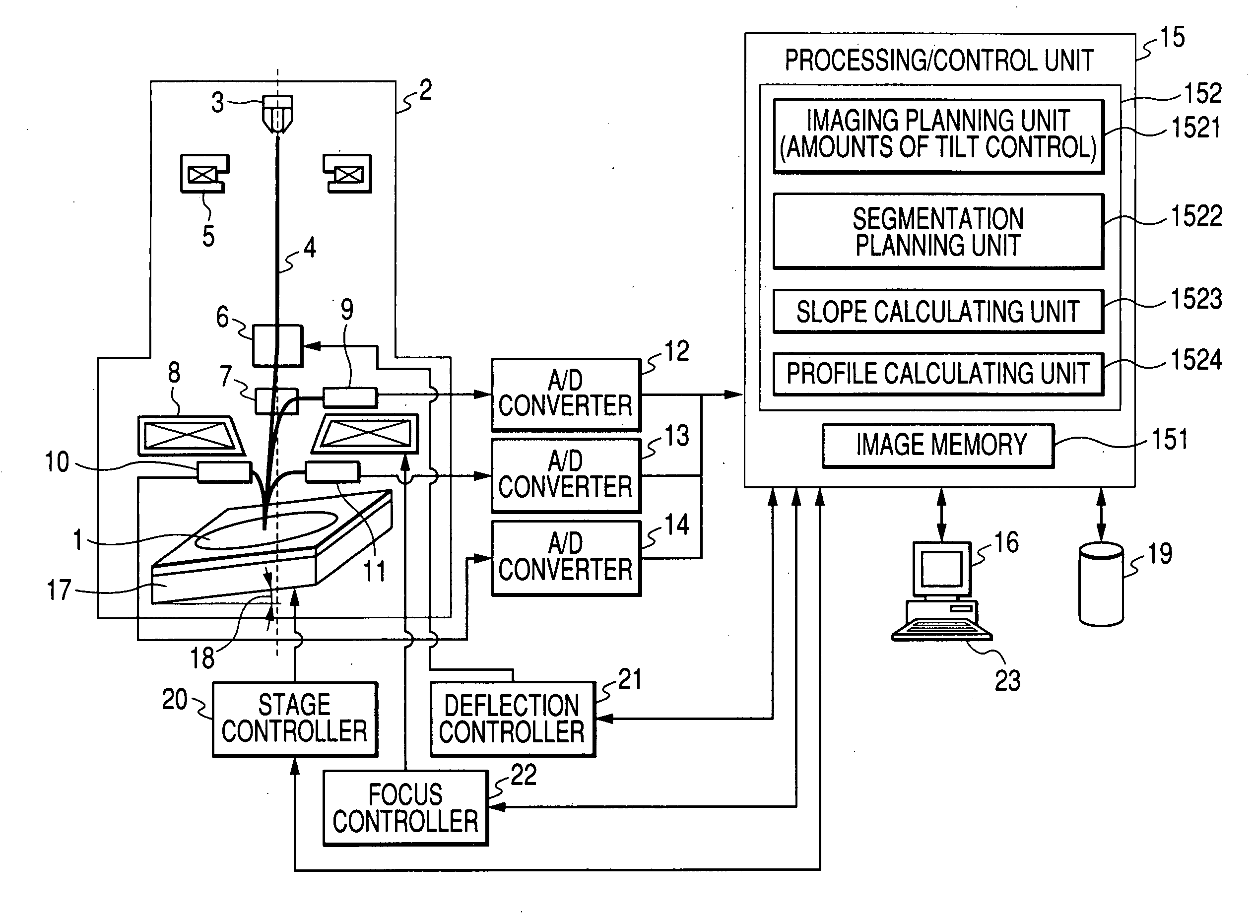
Figure 1 
Figure 2 
Figure 3
Abstract
Description
BACKGROUND OF THE INVENTION
[0001] The present invention relates to a method and apparatus for measuring or estimating the three-dimensional profile of a specimen such as a semiconductor wafer in a semiconductor manufacturing process based on images obtained by observing the specimen using an SEM (Scanning Electron Microscope) when the specimen is observed or measured.
[0002] With the miniaturization of semiconductor devices, the pre-process for manufacturing these devices is becoming increasingly difficult to control. The electrical characteristics of a semiconductor device pattern are very much affected by its height and line width and the inclination angles of the sidewalls, as well as minute pattern shape variations such as the roundness of the corners. As such, there has been a need to accurately measure these dimensions and shapes to detect process variations and thereby control the process. Thus, effectively controlling the manufacturing process of a semiconductor device requ...
Examples
Embodiment Construction
[0030] There will now be described methods and apparatuses for measuring a three-dimensional profile using an SEM (Scanning Electron Microscope) according to preferred embodiments of the present invention with reference to the accompanying drawings.
[0031]FIG. 1 is a diagram showing a system for obtaining and processing an SEM image according to an embodiment of the present invention. As shown in the figure, an electron optical system 2 comprises an electron beam source (an electron gun) 3 for emitting an electron beam 4, a condensing lens 5, a deflector 6, an ExB deflector 7, an objective lens 8, a secondary electron detector 9, and reflected electron detectors 10 and 11. Reference numeral 17 denotes a stage (X-Y-Z stage) on which a specimen 1 (e.g., a semiconductor wafer) is placed. The stage 17 includes a tilt stage for forming a stage tilt angle 18. It should be noted that the stage 17 can be tilted in the X- and Y-directions about tilt axes as a center which is substantially a ...