
Defect inspection method and apparatus
a defect inspection and defect technology, applied in image enhancement, instruments, image data processing, etc., can solve the problems of large pixel level error, inconsistent information, and inability to ensure the coincidentity of two images to be compared, so as to achieve high reliability of inspection and effectively make defect review. , the effect of ensuring inconsistent information
Patent Information
- Authority / Receiving Office
- US · United States
- Patent Type
- Applications(United States)
- Current Assignee / Owner
- Publication Date
- 2006-02-23
- Estimated Expiration
- Not applicable · inactive patent
Smart Images
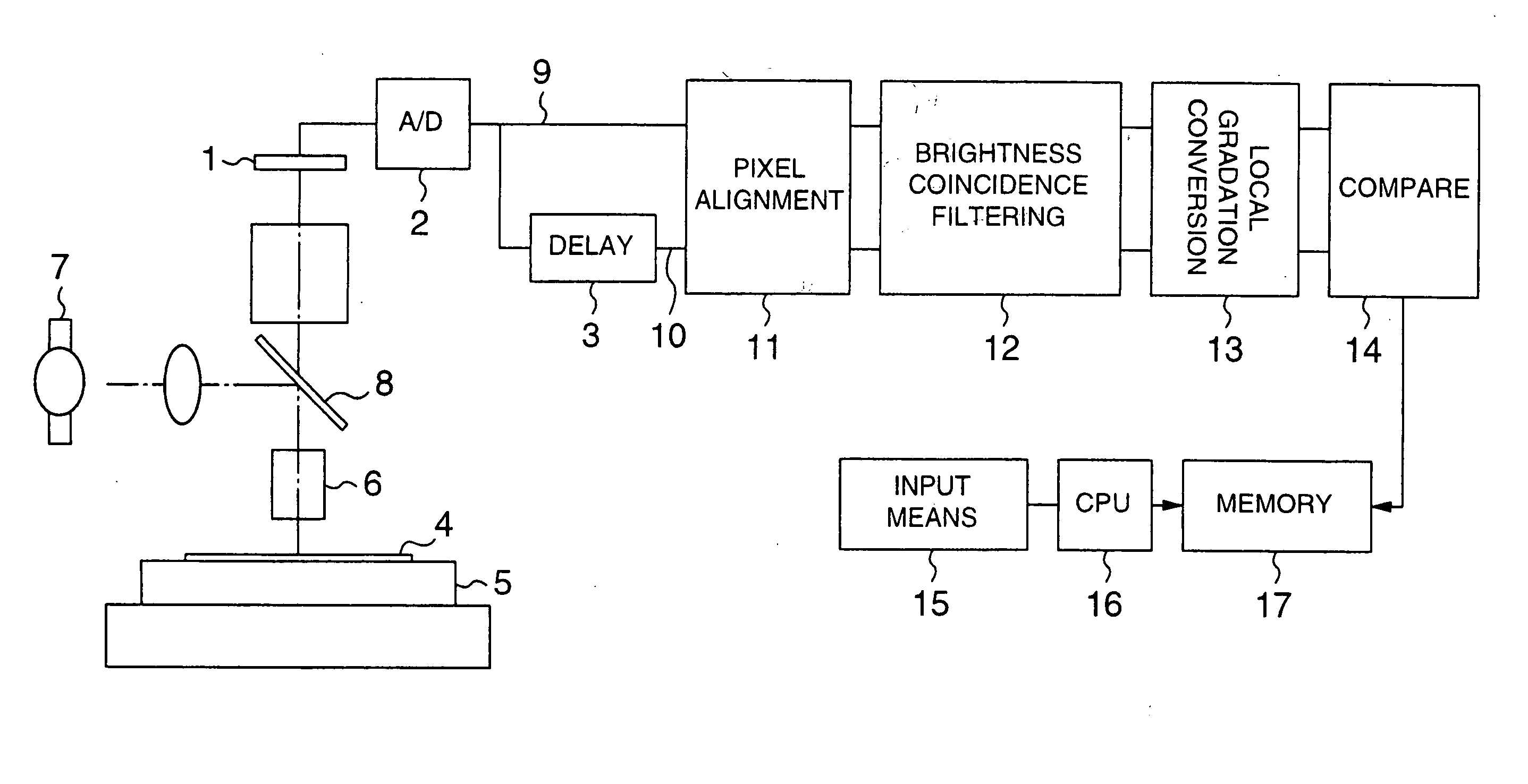
Figure 1 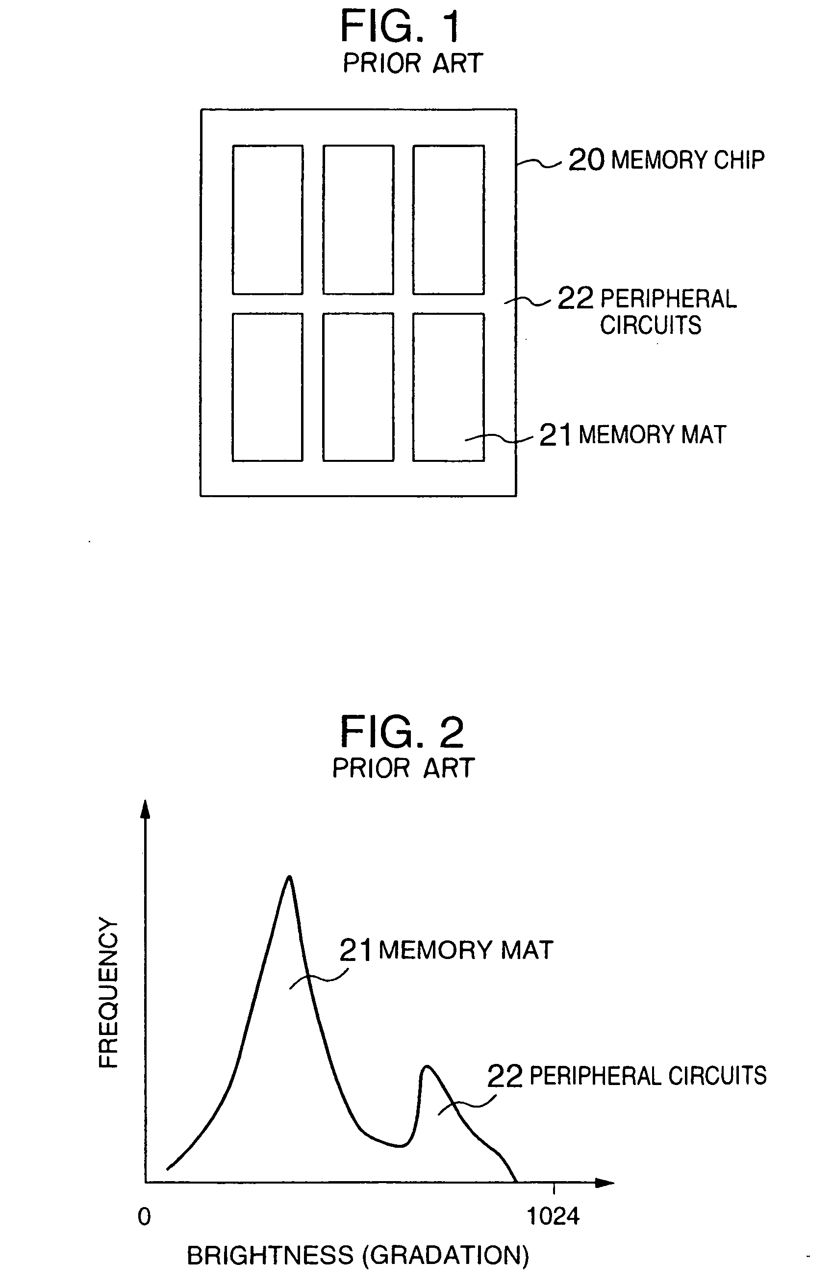
Figure 2 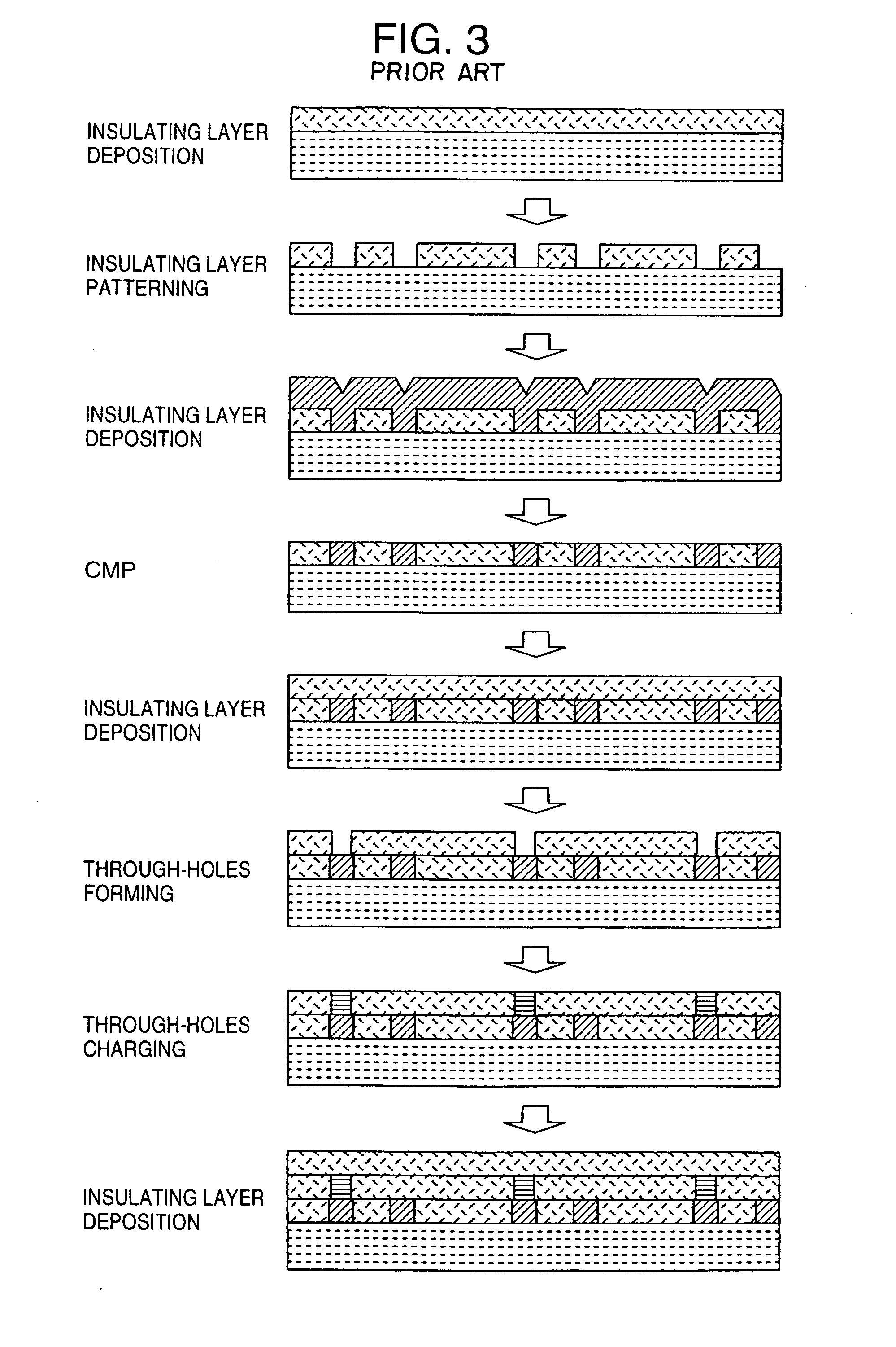
Figure 3
Abstract
Description
CROSS REFERENCE TO RELATED APPLICATIONS
[0001] This application is a continuation application of application Ser. No. 09 / 294,137, filed Apr. 20, 1999, based on Japanese Patent Application No. 10-110383, filed in Japan on Apr. 21, 1998 and No. 10-264275, filed Sep. 18, 1998, the contents of all of which are incorporated herein by reference in their entirety.BACKGROUND OF THE INVENTION
[0002] The present invention relates to exterior inspection for detecting defects of patterns being examined, and particularly to a defect inspection method and apparatus for inspecting patterns in a semiconductor wafer or liquid crystal display.
[0003] In a conventional inspection apparatus of this kind, as disclosed in JP-A-55-74409, an image sensor such as a line sensor is used to detect the image of a pattern being examined while the pattern is being moved, and the detected image signal is compared in its gradation with another image signal delayed by a predetermined time, so that the inconsistency ...
Examples
embodiment 1
[Embodiment 1]
[0052]FIGS. 7 and 8 are block diagrams of pattern defect inspection apparatus according to the first embodiment of the invention.
[0053] It is assumed that this embodiment inspects, for example, patterns of a semiconductor wafer.
[0054] Referring to FIGS. 7 and 8, there are shown an image sensor 1 that responds to the brightness or gradation of light reflected from a semiconductor wafer 4 of patterns being inspected to produce a gradation image signal, an A / D converter 2 for converting the gradation image signal from the image sensor 1 into a digital image signal 9, a delay memory 3 for delaying the gradation image signal, and the semiconductor wafer 4 having patterns being inspected. There are also shown a stage 5 that is moved in X-direction, Y-direction, Z-direction and θ-direction (rotation) with the semi-conductor wafer 4 placed thereon, an object lens 6 facing the semiconductor wafer 4, a light source 7 for illuminating the semiconductor wafer 4 of the patterns b...
embodiment 2
[Embodiment 2]
[0123]FIG. 24 shows the second embodiment of a pattern inspection method and apparatus according to the invention. In this embodiment, an electron beam is used to scan the sample and the electrons generated from the wafer by the irradiation of the electron beam are detected. An electron beam image of the scanned region is thus obtained on the basis of the change of the intensity, and used to make a pattern inspection. The second embodiment overcomes the problems to be solved by the invention by setting a defect decision threshold for each pixel considering pattern shift and different gradations.
[0124] This system includes a detection unit 101, an image extractor 102, an image processor 103, a whole controller 104 for controlling the whole system.
[0125] The detection unit 101 will be described first.
[0126] Referring to FIG. 24, an electron beam emitted from an electron gun 31 passes through a magnetic field lens 32 and an object lens 33 and focused on the sample surf...
embodiment 3
[Embodiment 3]
[0148]FIG. 26 shows the third embodiment of a pattern defect inspection method and apparatus according to the invention. Referring to FIG. 26, in which like elements corresponding to those in FIGS. 7 and 8 are provided, there are shown the image sensor 1 for producing a gradation image signal according to the brightness, or gradation of the reflected light from the semiconductor wafer 4 that has patterns being inspected, the A / D converter 2 for converting the gradation image signal from the image sensor 1 into the digital image signal 9, the delay memory 3 for delaying the gradation image signal, the semiconductor wafer 4 having the patterns being inspected, and the stage 5 on which the semiconductor wafer 4 of the patterns being inspected is placed and which is moved in the X-direction, Y-direction, Z-direction and θ-direction (rotation). In addition, there are shown the object lens 6 placed facing to the semiconductor wafer 4, the light source 7 for illuminating the ...