
Semiconductor device manufacturing method
Patent Information
- Authority / Receiving Office
- US · United States
- Current Assignee / Owner
- Publication Date
- 2006-05-11
- Estimated Expiration
- Not applicable · inactive patent
Smart Images
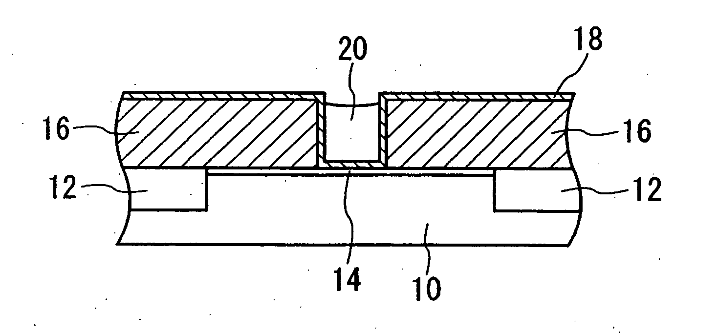
Figure 1 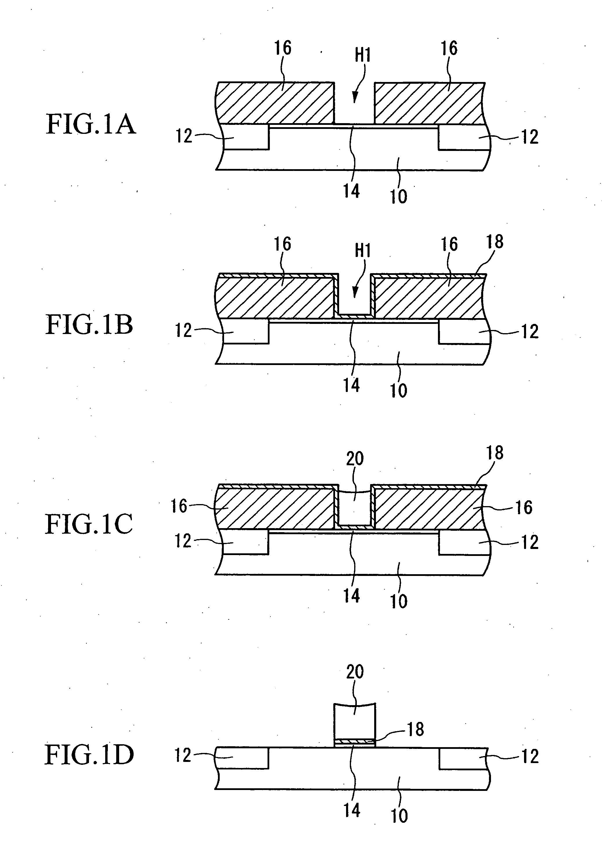
Figure 2 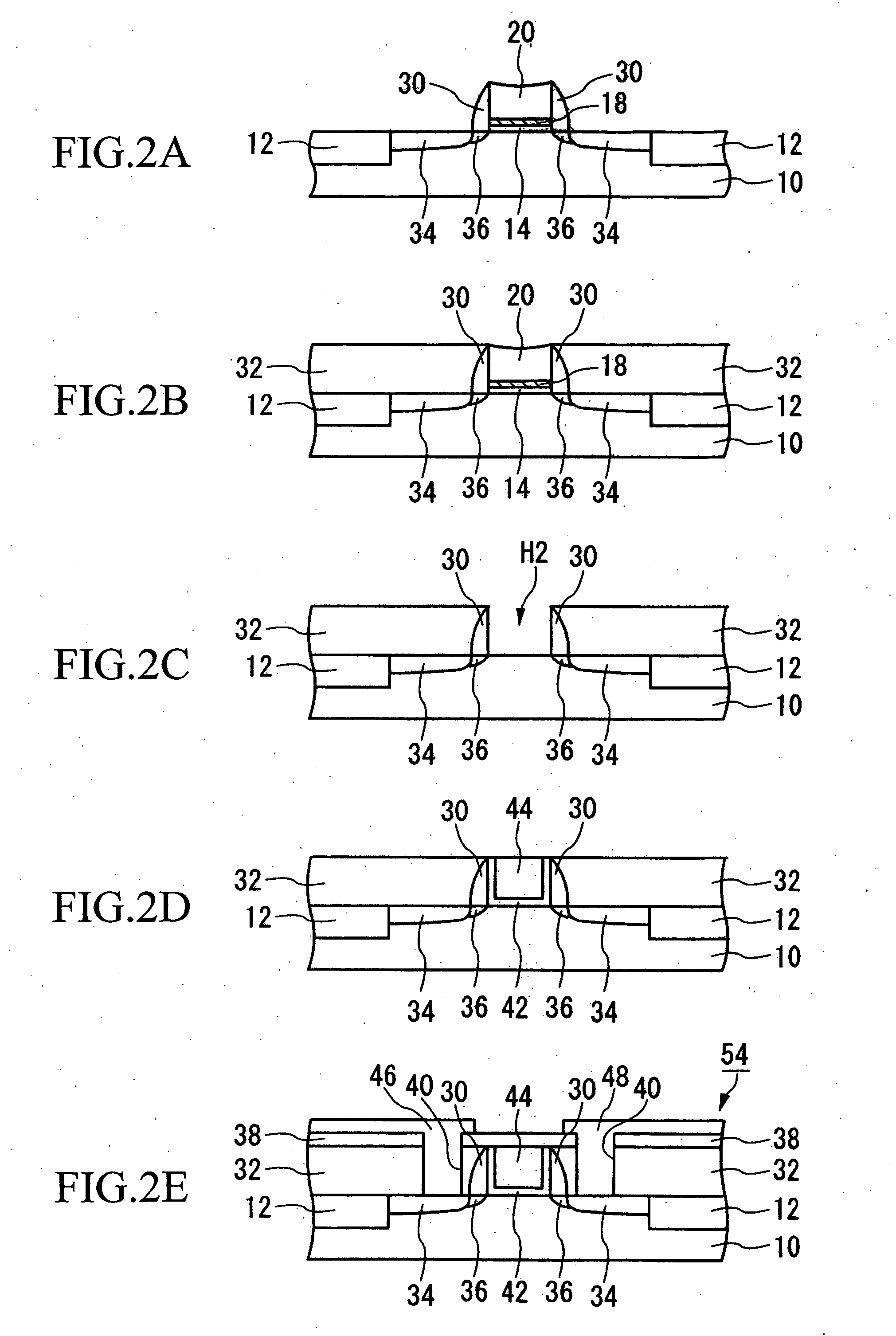
Figure 3
Abstract
Description
BACKGROUND OF THE INVENTION
[0001] 1. Field of the Invention
[0002] This invention relates to a method of manufacture of a semiconductor device.
[0003] Priority is claimed on Japanese Patent Application No. 2004-325070, filed Nov. 9, 2004, the content of which is incorporated herein by reference.
[0004] 2. Description of Related Art
[0005] LSI devices and other integrated circuits have been mounted in portable telephone sets, notebook-type personal computers, PDAs (Personal Digital Assistants), and other electronic equipment, in efforts to make electronic equipment more compact and provide sophisticated functions. Such LSI devices and other integrated circuits contain field effect transistors (MOSFETs), capacitors, resistors and similar, integrated and stacked on a semiconductor substrate.
[0006] However, trends toward greater compactness of electronic equipment in recent years have led to increased demands for smaller device components, and it has become increasingly necessary to r...
Examples
Embodiment Construction
[0030] Below, aspects of the invention are explained, referring to the drawings.
[0031] In one aspect, processes to manufacture a MOSFET having an LDD structure are explained, referring to the drawings. First, the processes to form a dummy gate pattern for use as a mask, when implanting impurities into silicon substrate in a prescribed concentration, are explained in detail. In each of the drawings used in the following explanation, the scales of the various members have been modified appropriately to a size enabling visual identification of the members.
[0032] -Method of Formation of Dummy Gate Pattern-
FIGS. 1A to 1D are cross-sectional views showing the processes for formation of a dummy gate pattern in this aspect.
[0033] First, as shown in FIG. 1A, a device separation film 12 is formed, to provide electrical insulation between adjacent devices. Specifically, a reactive ion etching (RIE) method or similar is used to form a shallow trench portion in the silicon substrate 10. This...