
Semiconductor device and manufacturing method thereof
Patent Information
- Authority / Receiving Office
- US · United States
- Current Assignee / Owner
- Publication Date
- 2007-05-10
- Estimated Expiration
- Not applicable · inactive patent
Smart Images
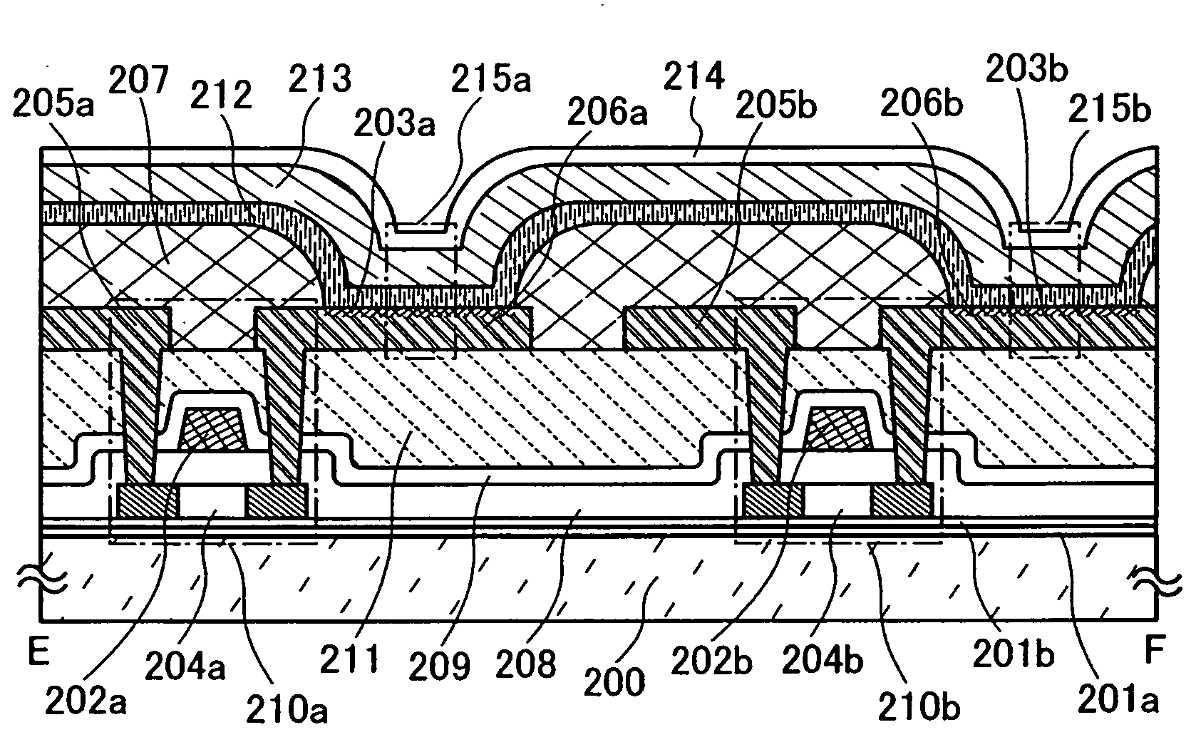
Figure 1 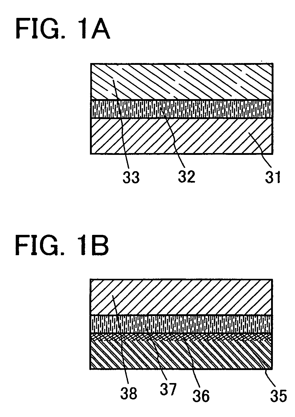
Figure 2 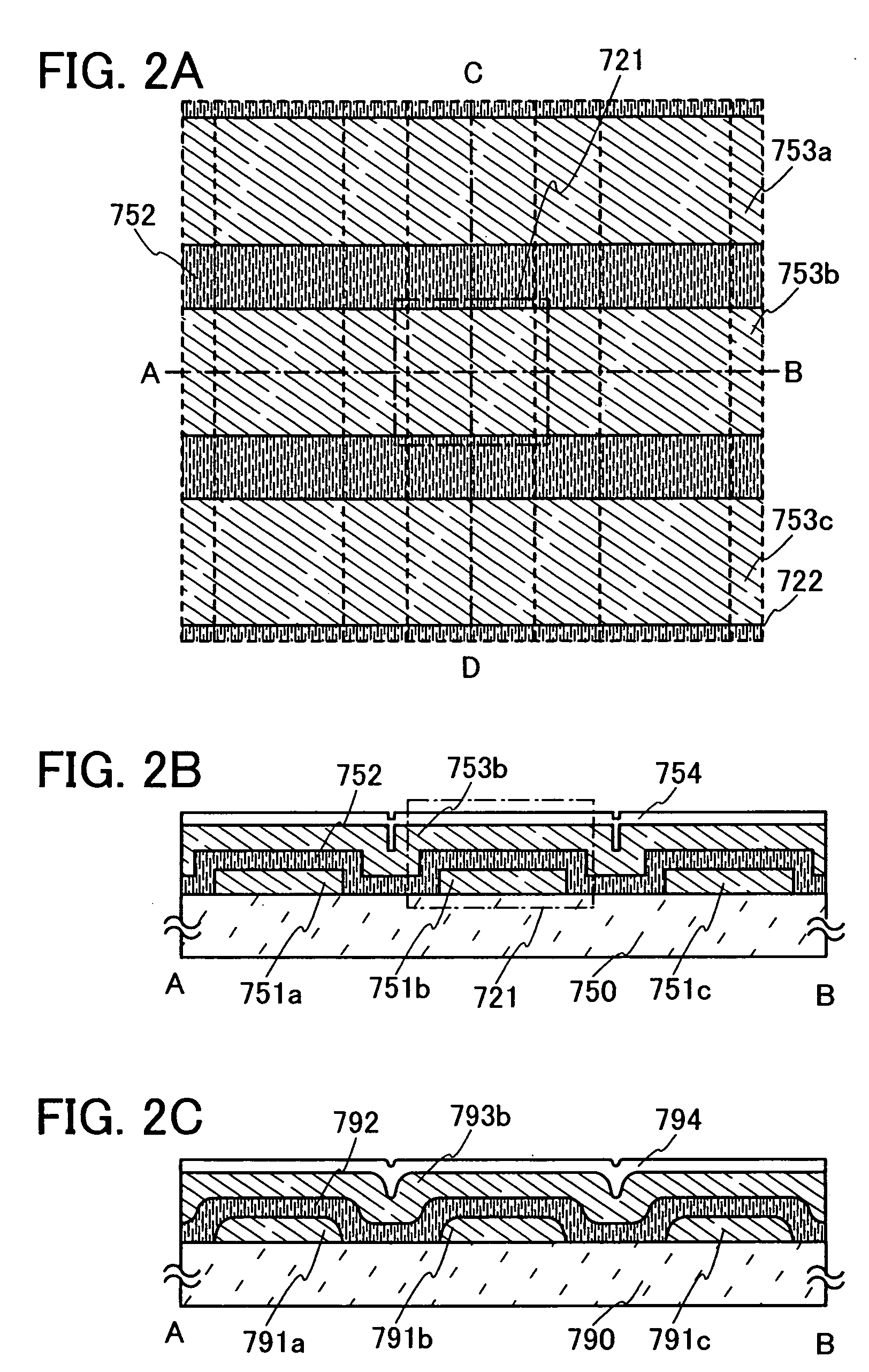
Figure 3
Abstract
Description
TECHNICAL FIELD
[0001] The present invention relates to a semiconductor device and a manufacturing method of the semiconductor device. BACKGROUND ART
[0002] Recently, an individual-recognition technique has drawn attention, in which by giving an ID (individual identification number) to each object, information such as a history of the object is clarified for manufacturing, management, or the like. In particular, a semiconductor device capable of non-contact data transmission and reception has been developed. As such a semiconductor device, an RFID (Radio Frequency Identification: also called an ID tag, an IC tag, an IC chip, an RF (Radio Frequency) tag, a wireless tag, an electronic tag, or a wireless chip) or the like specifically begins to be introduced into companies, markets, or the like.
[0003] Such a semiconductor device generally includes an antenna and a circuit (hereinafter, also referred to as an IC (Integrated Circuit) chip) using a semiconductor substrate of silicon (Si)...
Examples
embodiment mode 1
[0053] A memory element to which the present invention is applied will be described in this embodiment mode, using FIGS. 1A and 1B.
[0054] The invention focuses on adhesion between the organic compound layer and the first conductive layer and between the organic compound layer and the second conductive layer. Adhesion between substances is affected by the solubility parameter (SP value). Solubility parameter is a value of the ½-th power of the cohesive energy density (CED) of one molecule per unit volume.
[0055] As respective SP values of substances get closer to each other, adhesion between the substances is increased. In general, the SP value of an organic compound material is small as compared to that of a metal material. Therefore, for improving the adhesion between the organic compound layer and each conductive layer, an organic compound material having an SP value as large as possible may be selected for the organic compound layer whereas a metal material having an SP value as...
embodiment mode 2
[0115] In this embodiment mode, one structural example of the memory element included in the semiconductor device of the present invention will be described using the drawings. In particular, the case where the semiconductor device is a passive matrix type will be described.
[0116] The memory element of the present invention and an operation mechanism thereof are described using FIGS. 2A to 2C, 6A, and 6B. The memory element in this embodiment mode can be manufactured by the same material and with the same structure as those in Embodiment Mode 1, and therefore, detailed description of the material or the like is omitted here.
[0117]FIGS. 3A to 3C each show one constitution example of the semiconductor device of the invention, which include a memory cell array 722 including memory cells 721 provided in matrix, a circuit 726 including a reading circuit and a writing circuit, a decoder 724, and a decoder 723. It is to be noted that the constitution of a semiconductor device 716 shown h...
embodiment mode 3
[0135] In this embodiment mode, a semiconductor device having constitution different from that of Embodiment Mode 2 will be described. In particular, the case where the semiconductor device is an active matrix type will be described. A memory element in this embodiment mode can be manufactured by using the same material and with the same structure as that in Embodiment Mode 1, and therefore, detailed description of the material or the like is omitted here.
[0136]FIGS. 5A to 5C show one constitution example of the semiconductor device of this embodiment mode, which include a memory cell array 232 including memory cells 231 in matrix, a circuit 226, a decoder 224, and a decoder 223. The circuit 226 includes a reading circuit and a writing circuit. It is to be noted that the constitution of a semiconductor device 217 shown here is only one example; the semiconductor device may include another circuit such as a sense amplifier, an output circuit, or a buffer, and the writing circuit may...