
Varistor
a varistor and resistance value technology, applied in the field of varistor, can solve problems such as impairment of varistor characteristics, and achieve the effects of improving durability and reliability, preventing fluctuations in the resistance value of varistor, and improving bonding strength
Patent Information
- Authority / Receiving Office
- US · United States
- Patent Type
- Applications(United States)
- Current Assignee / Owner
- Publication Date
- 2009-06-25
Smart Images
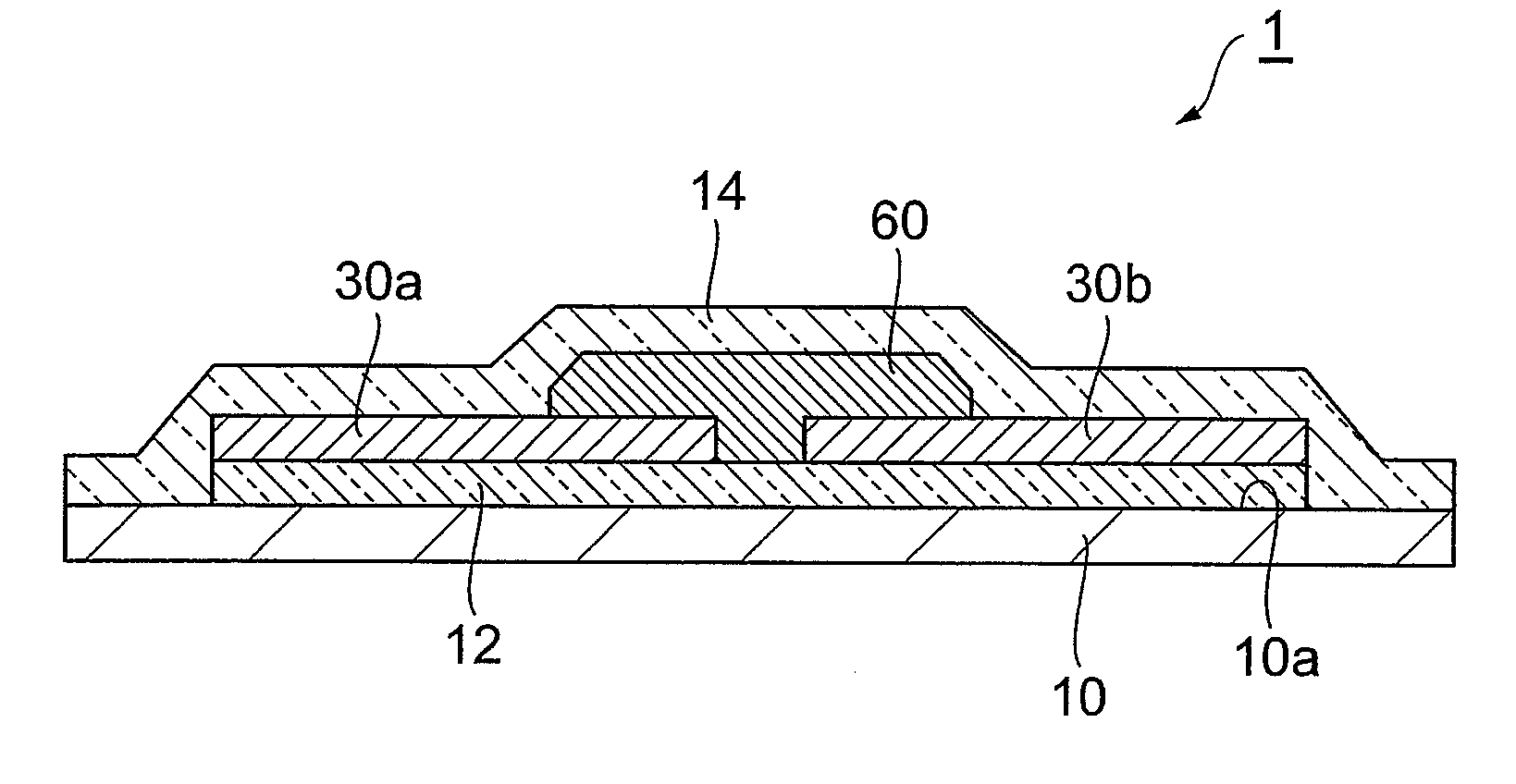
Figure 1 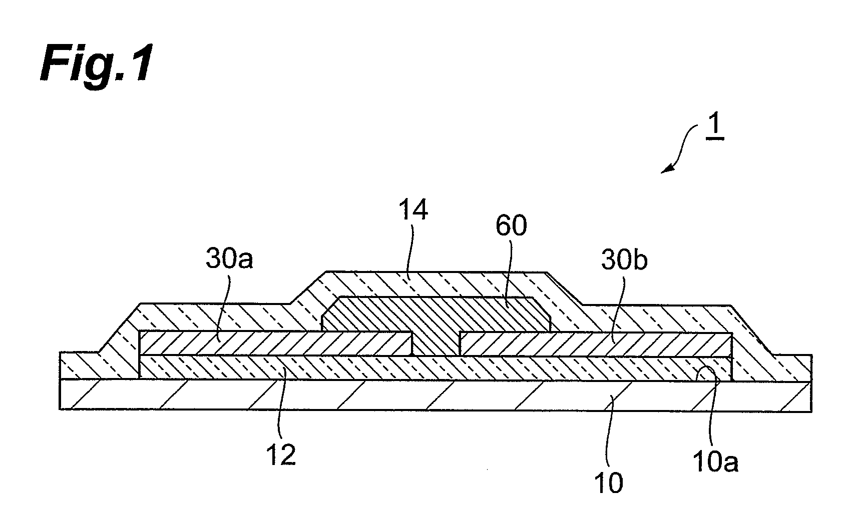
Figure 2 
Figure 3
Abstract
Description
BACKGROUND OF THE INVENTION
[0001] 1. Field of the Invention
[0002] The present invention relates to a varistor integrally comprising a resistor and a varistor element.
[0003] 2. Related Background Art
[0004] Varistors are used in, for example, controlling devices, communication devices and their parts, to absorb or eliminate external surges (abnormal voltage) such as static electricity or noise, for protection against such external surges or noise.
[0005] The use of zinc oxide as a major component and rare earth elements, calcium oxide and silicon oxide as accessory components has been proposed for the constituent components of varistor elements in varistors, in order to enhance the varistor characteristics such as voltage non-linearity, as well as the discharge withstand current rating (see Japanese Patent Publication No. 3493384, for example).
[0006] Serial connection of resistors in a varistor requires separate mounting of two elements on the printed board, and thus increases the mounting s...
Examples
first embodiment
[0029]FIG. 1 is a schematic cross-sectional view of a varistor according to a first embodiment of the invention. In the varistor 1, a base glass layer 12 is laminated in contact with one main side 10a of a varistor element 10. A pair of external electrodes 30a, 30b is provided in contact with the main side of the base glass layer 12 opposite the varistor element 10 side. A resistor 60 is also provided in contact with the main side. That is, the pair of external electrodes 30a, 30b and the resistor 60 are both formed on the same main side of the base glass layer 12. The resistor 60 is formed provided in such a manner as to connect the pair of external electrodes 30a, 30b. At least part of the resistor 60 is formed between the pair of external electrodes 30a, 30b. The resistor 60 is also formed so as to cover portions of the sides of the pair of external electrodes 30a, 30b opposite the base glass layer 12 sides (the resistor 60 sides). The varistor 1 has a protective layer (overglaze...
second embodiment
[0060]A varistor according to a second embodiment of the invention will now be explained with reference to FIGS. 4 to 8. The varistor of this embodiment is a stacked chip varistor.
[0061]FIG. 4 is a schematic top view of a stacked chip varistor according to the second embodiment. FIG. 5 is a schematic bottom view of a stacked chip varistor according to the second embodiment. FIG. 6 is a diagram showing the cross-sectional structure along line VI-VI in FIG. 5. FIG. 7 is a diagram showing the cross-sectional structure along line VII-VII in FIG. 5. FIG. 8 is a diagram showing the cross-sectional structure along line VIII-VIII in FIG. 5.
[0062]As shown in FIGS. 4 to 8, the stacked chip varistor 21 comprises a roughly rectangular tabular varistor element 23, a plurality (25 according to this embodiment) external electrodes 25-29 formed on one main side (the lower side) 23a of the varistor element 23, and a plurality (20 according to this embodiment) external electrodes 30a-30d formed on th...
example 1
Preparation of Slurry for Varistor Element
[0097]First, a starting powder was prepared containing zinc oxide as the main component and the components listed in Table 1 as accessory components. The contents in Table 1 are proportions with respect to zinc oxide. The starting powder, organic binder, organic solvent and additives were mixed and crushed for 20 hours using a ball mill to obtain a slurry for the varistor element.
TABLE 1CompoundProportion (atomic %)SiO27.11K2O0.04CaO20.31Cr2O30.05Co3O40.70Pr6O110.09The proportions of the compounds in the table are values based on the metal or metalloid atoms.
[0098]
[0099]A conductive paste was prepared containing the components for “Electrode A” listed in Table 2. Specifically, each of the components of the “Electrode A” shown in Table 2 were mixed in the proportions shown in Table 2 to prepare a starting mixture.
[0100]The starting mixture was mixed with the organic binder and organic solvent for 20 hours using a ball mill to obtain a conduct...