
Method of mounting electronic circuit constituting member and relevant mounting apparatus
a technology of electronic circuit and mounting apparatus, which is applied in the direction of printed circuit manufacturing, coating, conductive pattern formation, etc., can solve the problems of high manufacturing cost, high manufacturing cost, and the inability to form crystalline semiconductor transistors on glass substrates, etc., and achieves accurate mounting and good reproducibility
Patent Information
- Authority / Receiving Office
- US · United States
- Patent Type
- Applications(United States)
- Current Assignee / Owner
- Publication Date
- 2009-10-29
- Estimated Expiration
- Not applicable · inactive patent
Smart Images
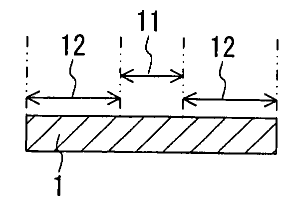
Figure 1 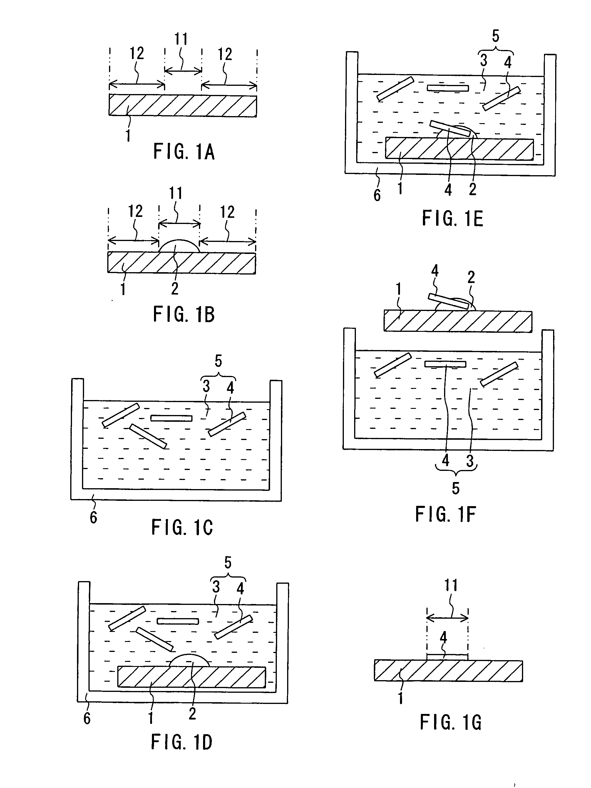
Figure 2 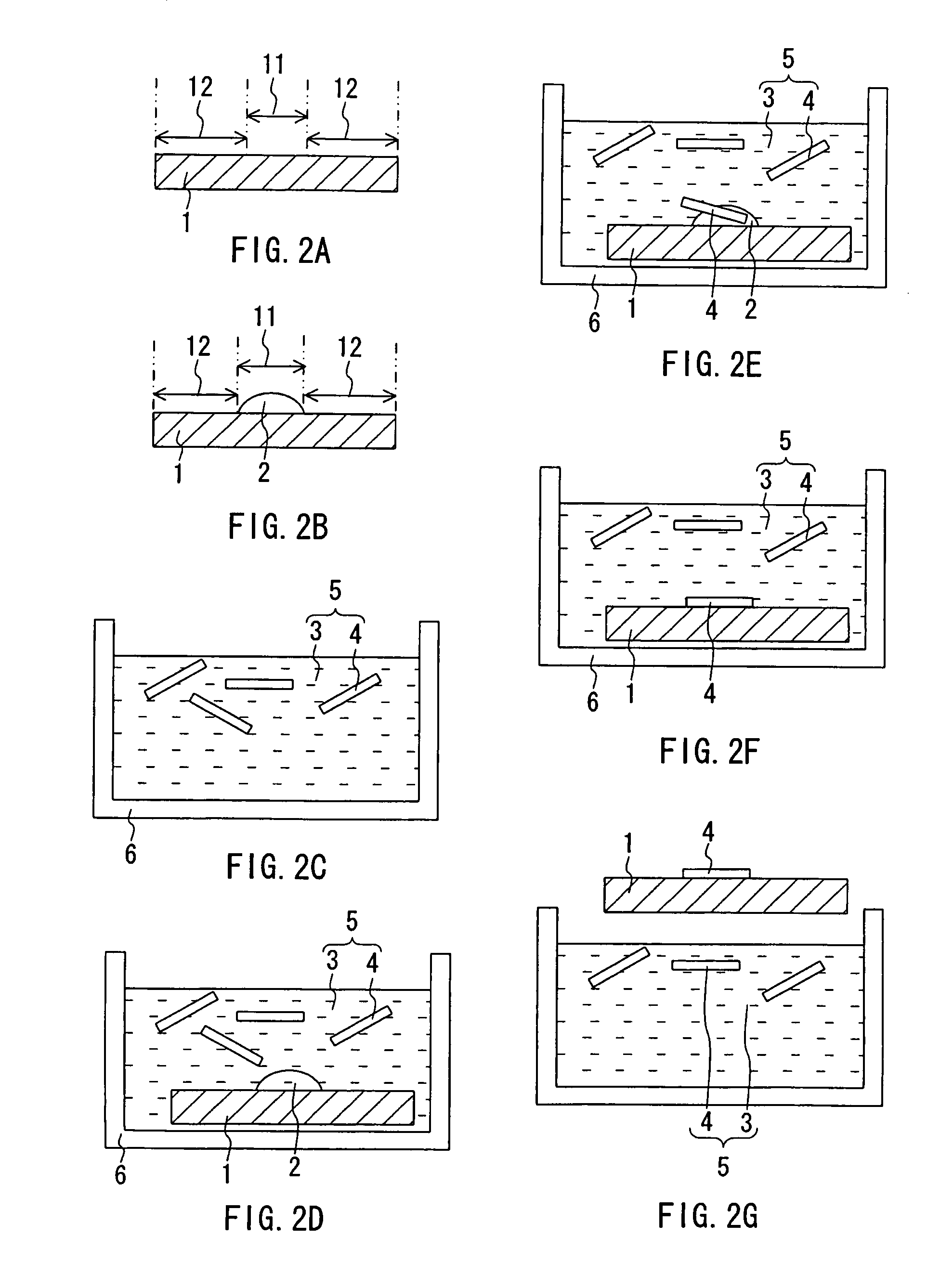
Figure 3
Abstract
Description
TECHNICAL FIELD
[0001] The present invention relates to a method and apparatus for mounting electronic circuit-constituting members.BACKGROUND ART
[0002] Active-matrix liquid crystal display elements and organic electroluminescence display elements are formed on a glass substrate. The pixels disposed in a matrix on the substrate are controlled by the transistors provided in the vicinity of the pixels. With current technology, however, crystalline semiconductor transistors cannot be formed on the glass substrate, and for this reason thin film transistors formed of an amorphous silicon or polysilicon thin film have been used for the control of the pixels. The thin film transistor has the advantage that it can be formed on a large-area substrate at low cost; however, its smaller mobility compared with crystalline silicon has prevented them from operating at high speed. To overcome such a problem, there have been proposed techniques in which the transistors first are fabricated on a silicon...
Examples
first embodiment
[0121]In the First Embodiment, a mounting method of the present invention will be described in detail with reference to the drawings. In the present embodiment, the description will be directed to the case where the electronic circuit-constituting member is a component chip including an electronic device, and the component chip is mounted on a substrate.
[0122]FIG. 1A to FIG. 1G, and FIG. 3A and FIG. 3B schematically illustrate respective steps of a mounting method of the present embodiment. First, a substrate 1 as shown in FIG. 1A and FIG. 3A is prepared. On one principal surface of the substrate 1 are provided a first region 11 and a second region 12 surrounding the first region 11. The first region 11 and the second region 12 are formed such that the first region 11 is more wettable than the second region 12 with respect to the first liquid described later. As shown in FIG. 3A, the first region 11 is rectangular in shape. In the following, the surface of the substrate 1 provided w...
second embodiment
[0168]In the Second Embodiment below, the description is directed to a fabrication method of an electronic instrument of the present invention, and a display device fabricated by the fabrication method, with reference to the drawings. The following description of the present embodiment will be given based on a fabrication method of a display device, or more specifically a liquid crystal display, as an example of the electronic instrument. It should be noted that the present invention is not limited by the following description.
[0169]FIG. 14 schematically illustrates a partial configuration of a liquid crystal display 140 as an electronic instrument of the present embodiment.
[0170]The liquid crystal display 140 includes a glass substrate 141, an X driver 142, a Y driver 143, X scanning electrodes 144, Y scanning electrodes 145, transistor chips (component chips) 146, and pixel portions 147. The transistor chips 146 are monocrystalline silicon transistors.
[0171]The pixel portions 147 ...
third embodiment
[0191]In the Third Embodiment below, the description is directed to a fabrication method of an electronic instrument of the present invention, and a display device fabricated by the fabrication method, with reference to the drawings. The description of the present embodiment will be given based on a fabrication method of a display device, or more specifically an organic electroluminescence display (organic EL display) as an example of an electronic instrument. The present invention is not limited by the following description.
[0192]FIG. 17 schematically illustrates a configuration of an organic EL display 200 of the present embodiment.
[0193]The organic EL display 200 includes a substrate 201 made of polycarbonate, an X driver 202, a Y driver 203, X scanning electrodes 204, Y scanning electrodes 205, component chips 206 and pixel portions 207. The component chips 206 each include a crystalline silicon transistor circuit. The pixel portions 207 include organic EL material, and are cont...