
Self aligned double patterning flow with non-sacrificial features
a double patterning and self-aligning technology, applied in the direction of basic electric elements, semiconductor/solid-state device manufacturing, electric devices, etc., can solve the problem that the photolithographic technique may not reliably form, and achieve the effect of reducing the number of processing steps and reducing the number of steps involved
Patent Information
- Authority / Receiving Office
- US · United States
- Patent Type
- Applications(United States)
- Current Assignee / Owner
- Publication Date
- 2010-06-03
- Estimated Expiration
- Not applicable · inactive patent
Smart Images
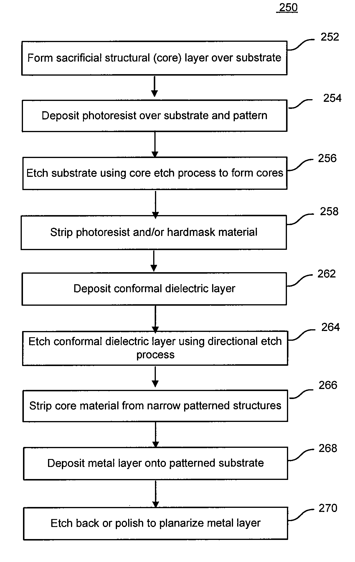
Figure 1 
Figure 2 
Figure 3
Abstract
Description
BACKGROUND
[0001] The application relates generally to substrate processing methods and particularly to process sequences which increase the density of features on the substrate.
[0002] Shrinking integrated circuits (ICs) may result in improved performance, increased capacity and / or reduced cost. Each device shrink requires more sophisticated techniques to form the features. Photolithography is commonly used to pattern features on a substrate. An exemplary feature is a line of a material which may be a metal, semiconductor or insulator. Linewidth is the width of the line and the spacing is the distance between adjacent lines. Pitch is defined as the distance between a same point on two neighboring lines. The pitch is equal to the sum of the linewidth and the spacing. Due to factors such as optics and light or radiation wavelength, however, photolithography techniques have a minimum pitch below which a particular photolithographic technique may not reliably form features. Thus, the minim...
Examples
Embodiment Construction
[0015]Embodiments of the present invention pertain to methods of forming features on a substrate using a self-aligned double patterning (SADP) process. A conformal layer of non-sacrificial material is formed over features of sacrificial structural material patterned near the optical resolution of a photolithography system using a high-resolution photomask. An anisotropic etch of the non-sacrificial layer leaves non-sacrificial ribs above a substrate. A gapfill layer deposited thereon may be etched or polished back to form alternating fill and non-sacrificial features. No hard mask is needed to form the non-sacrificial ribs, reducing the number of processing steps involved.
[0016]In order to better understand and appreciate the invention, reference is made to FIG. 2, which is a flowchart depicting steps associated with a self-aligned double patterning process according to one embodiment of the invention, and FIGS. 3A-F, which illustrate cross-sectional views of a structure as it is fo...