
Multilayer reflective film coated substrate, reflective mask blank, and method of manufacturing a reflective mask
a reflective film and substrate technology, applied in the field of multi-layer reflective film coated substrates, reflective mask blanks, and manufacturing methods, can solve the problems of difficult to avoid m, low position accuracy, and remarkable photolithography process used in semiconductor manufacturing processes, etc., to achieve accurate avoidance, high accuracy, and sufficient contrast
Patent Information
- Authority / Receiving Office
- US · United States
- Patent Type
- Applications(United States)
- Current Assignee / Owner
- Publication Date
- 2011-09-08
Smart Images
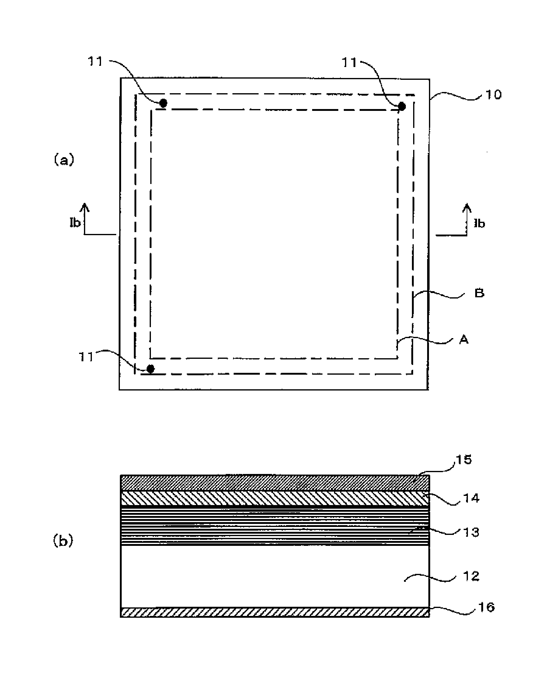
Figure 1 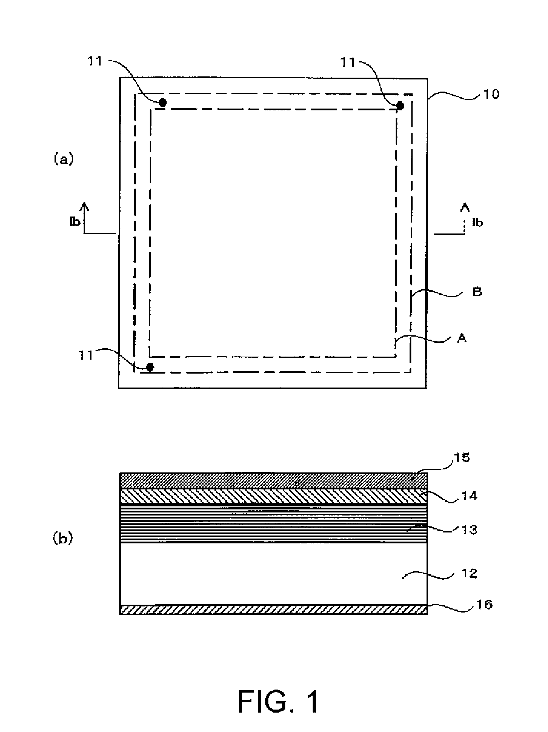
Figure 2 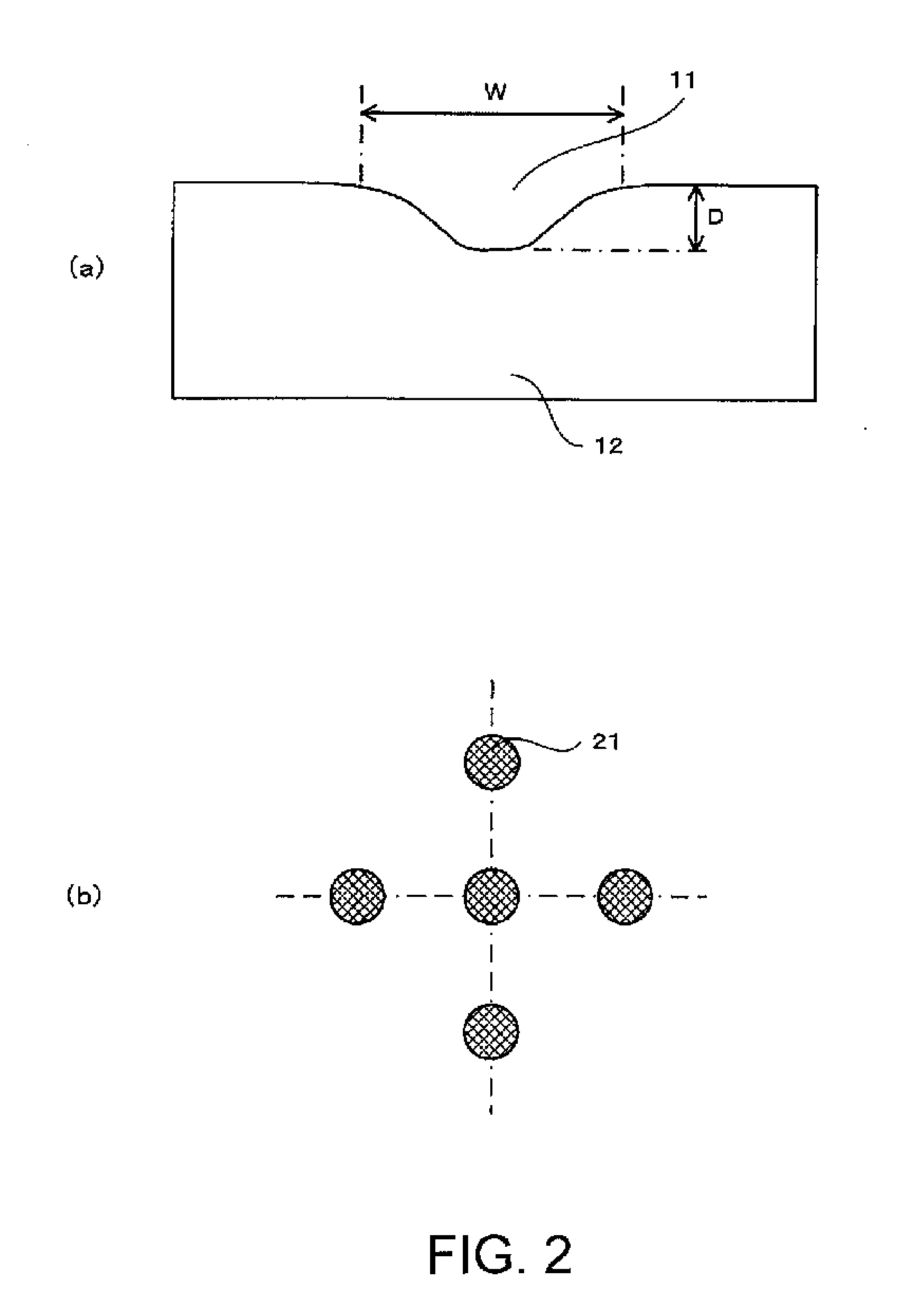
Figure 3
Abstract
Description
TECHNICAL FIELD
[0001] This invention relates to a multilayer reflective film coated substrate, a reflective mask blank, and a method of manufacturing a reflective mask.BACKGROUND ART
[0002] In recent years, with higher integration of semiconductor devices, patterns finer than the transfer limit of the photolithography technique using the conventional ultraviolet light have been required in the semiconductor industry. In order to enable transfer of such fine patterns, the EUV lithography being an exposure technique using extreme ultraviolet light (hereinafter referred to as EUV light) with a shorter wavelength is expected to be promising. Herein, the EUV light represents light in a wavelength band of the soft X-ray region or the vacuum ultraviolet region and, specifically, light having a wavelength of about 0.2 nm to 100 nm.
[0003] As an exposure mask for use in this EUV lithography, use is normally made of a reflective mask in which a multilayer reflective film (multilayer film) for refl...
Examples
examples 1 to 5
[0034]Hereinbelow, as Examples 1 to 5, there are shown the results of manufacturing reflective mask blanks each using a glass substrate having a reference point mark of the shape shown in FIG. 2 and examining whether identification of each reference point mark is good or bad.
[0035]First, a glass substrate of 6-inch square (152.4 mm×152.4 mm×6.35 mm) was used as a substrate and a reference point mark was formed in an area outside of a 132 mm square area (this area is a transfer pattern area) with respect to the center of a substrate main surface and inside of a 142 mm square area. This is because the area inside of 132 mm square is an area where a transfer pattern is to be formed, while, in the area outside of 142 mm square, the flatness is not good so that there is a possibility of the occurrence of position offset or the like upon forming the reference point mark.
[0036]As the reference point mark, a recess was formed using the carbon dioxide laser described above. By changing the i...