
Variable gain amplifier circuit
a gain amplifier and variable gain technology, applied in amplifiers, amplifiers with semiconductor devices/discharge tubes, amplifiers, etc., can solve the problems of large apparatus size, inability to achieve desired gain, and attenuation of input signal level, so as to achieve high accuracy gain adjustment, suppress the effect of input impedance change caused by gain chang
Patent Information
- Authority / Receiving Office
- US · United States
- Patent Type
- Applications(United States)
- Current Assignee / Owner
- Publication Date
- 2012-08-16
Smart Images
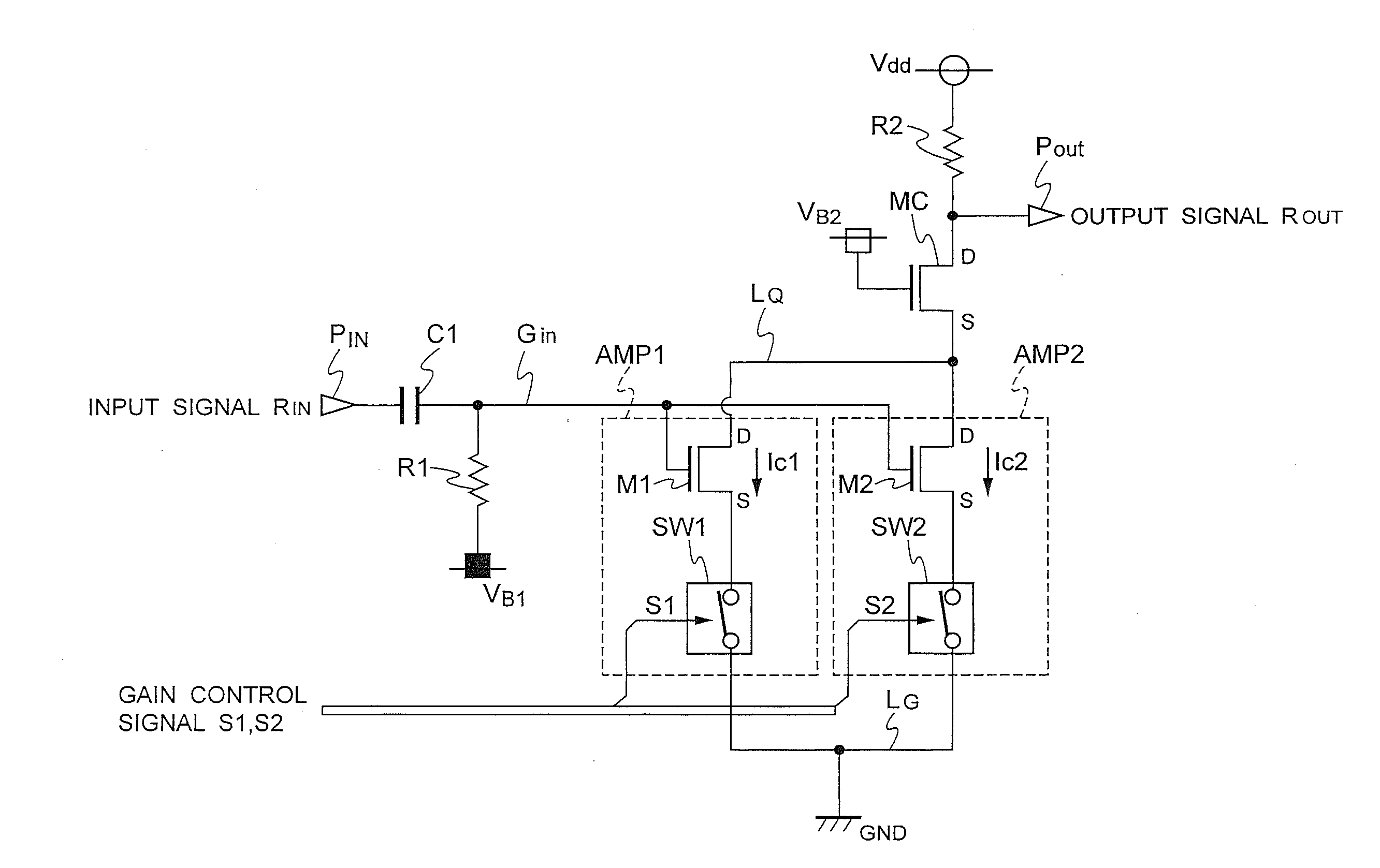
Figure 1 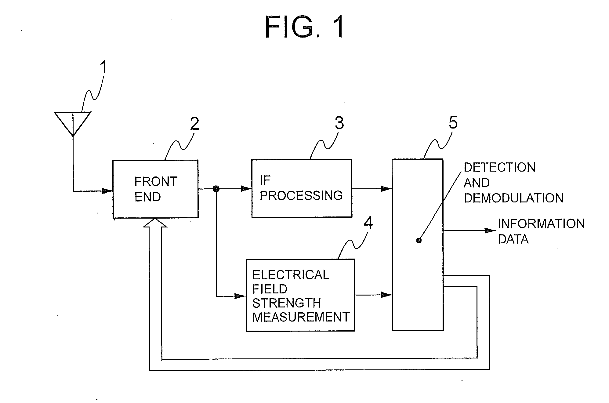
Figure 2 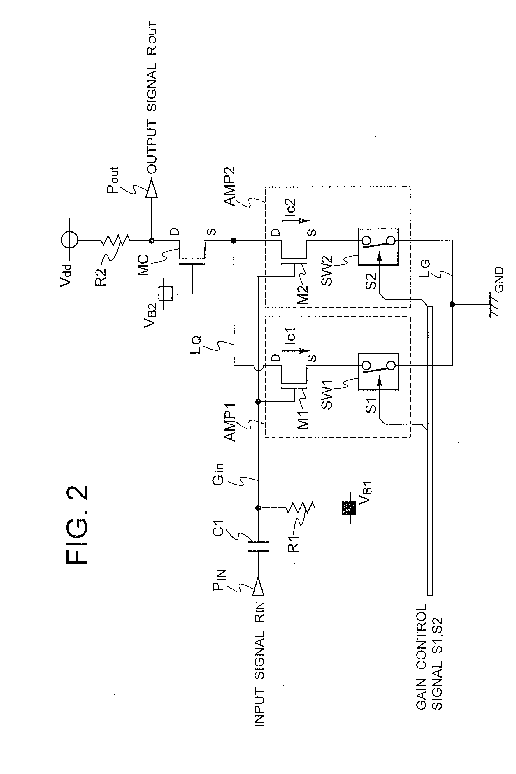
Figure 3
Abstract
Description
BACKGROUND OF THE INVENTION
[0001] 1. Technical Field
[0002] The present invention relates to a variable gain amplifier circuit that amplifies an input signal at variable gain.
[0003] 2. Description of the Related Art
[0004] A receiver used in wireless mobile communications is, at its front end, provided with a variable gain amplifier circuit that varies a gain according to the level of a received signal in order to maintain the level of the received signal at a constant level even when radio attenuation is caused by, for example, the distance between the receiver and the base station and existence of an obstacle therebetween.
[0005] A variable gain amplifier circuit with a wider variable gain range is proposed (see FIG. 1 of Patent Literature 1). In the configuration of this circuit, collector terminals of a plurality of amplification transistors (Q1 to Qn), i.e., transistors that amplify a received signal, are connected with each other.
[0006] The base terminals of the amplification transisto...
Examples
Embodiment Construction
[0019]In the variable gain amplifier circuit according to the present invention, a plurality of amplification portions are connected with each other in parallel between an amplification coupling line and a grounding line. The amplification portion includes a switching device and an amplification transistor, which induces a current corresponding to an input signal to flow between the amplification coupling line and the grounding line via the switching device when the switching device is in the on state. The amplitude gain is varied by, according to a gain control signal, separately switching on or off the switching devices of the respective amplification portions.
[0020]FIG. 1 is a block diagram illustrating a general configuration of a wireless receiver including a variable gain amplifier circuit according to the present invention.
[0021]In FIG. 1, a front end 2 amplifies a received signal received by an antenna 1, converts the signal into an intermediate frequency signal, and supplie...