
Method for manufacturing semiconductor device, resin sealing apparatus, and semiconductor device
Patent Information
- Authority / Receiving Office
- US · United States
- Current Assignee / Owner
- Publication Date
- 2013-01-24
- Estimated Expiration
- Not applicable · inactive patent
Smart Images
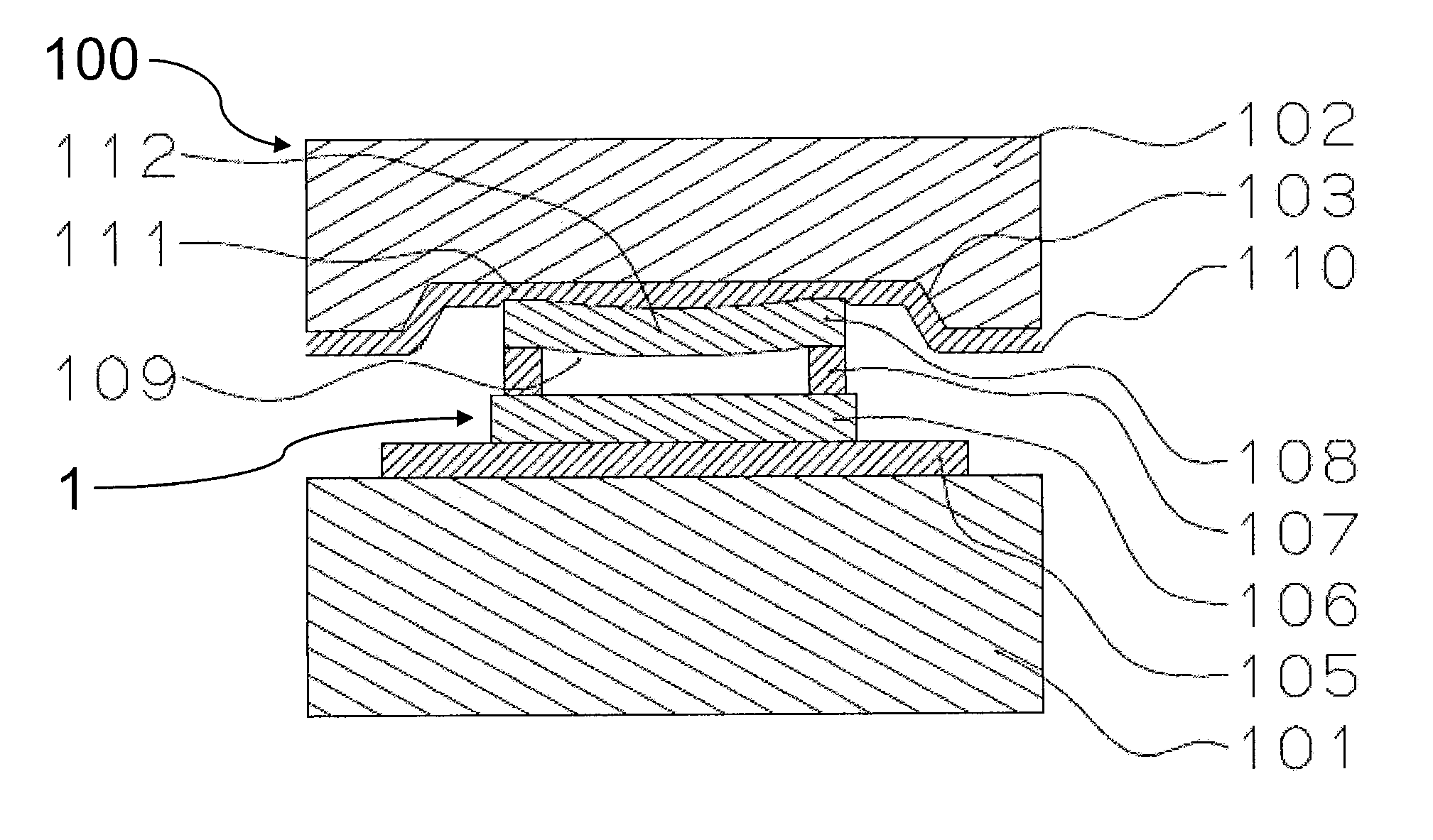
Figure 1 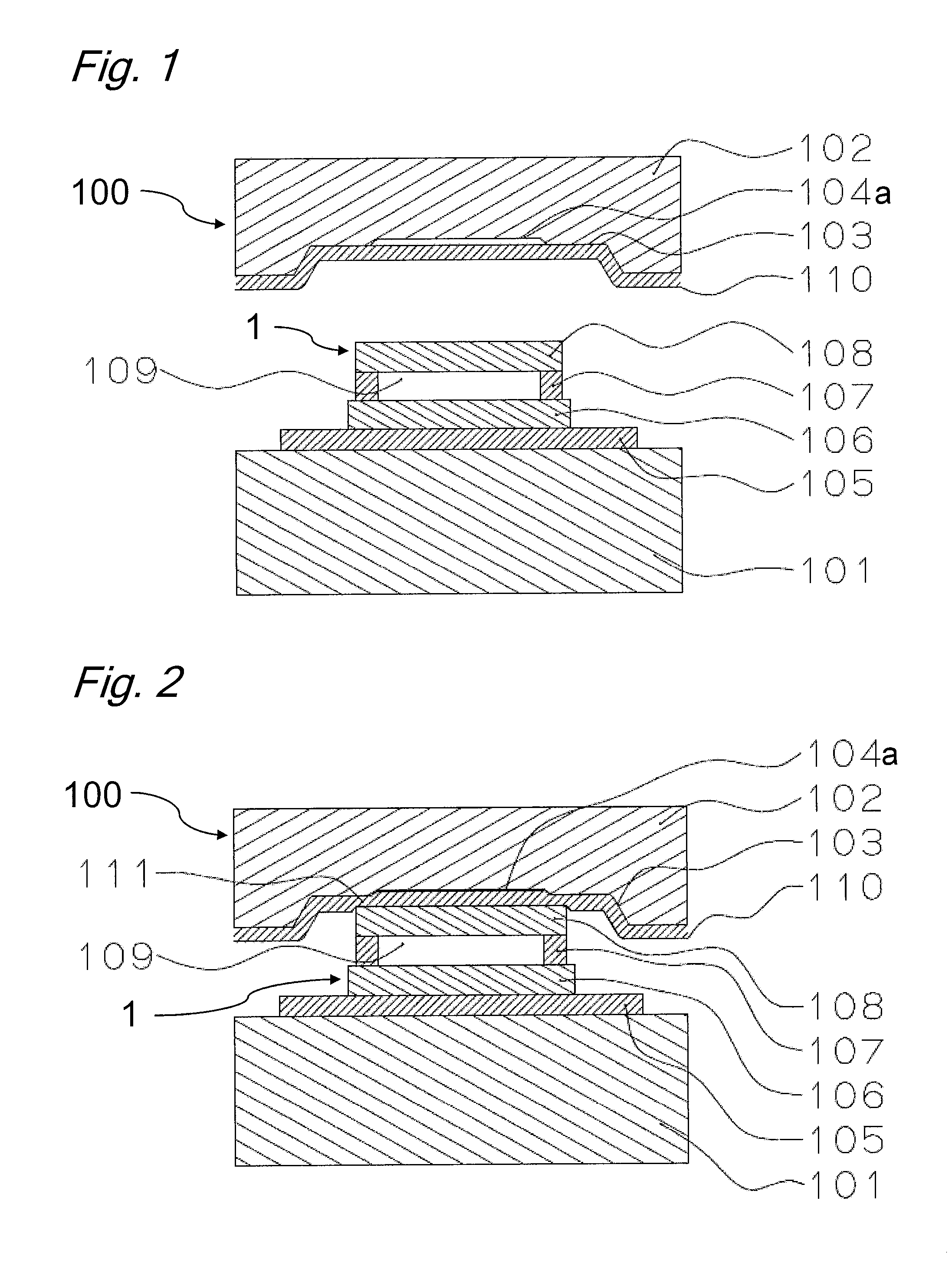
Figure 2 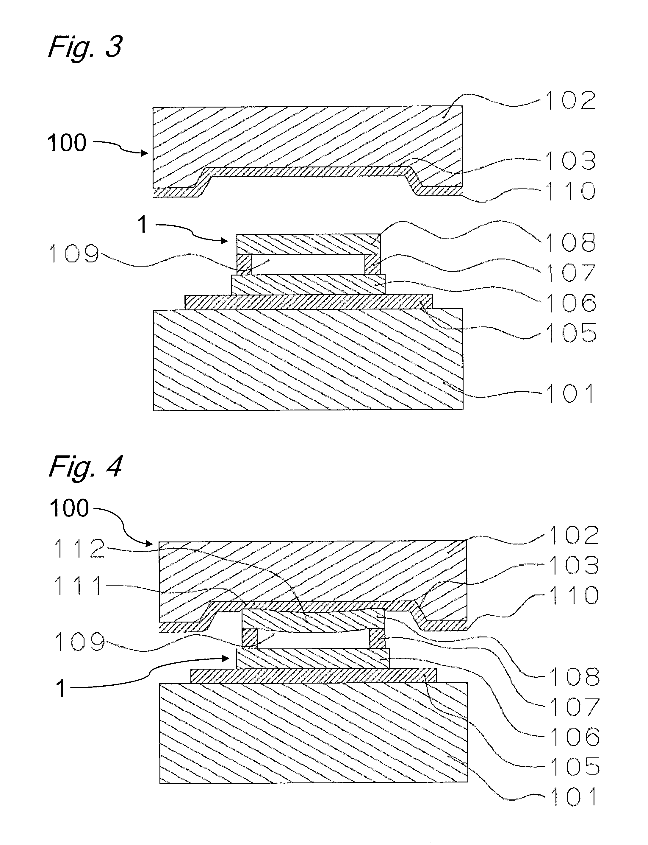
Figure 3
Abstract
Description
TECHNICAL FIELD
[0001] The present invention relates to a method for manufacturing a semiconductor device, and in particular, to a method for manufacturing a semiconductor device, in which a resin is molded on a semiconductor device having a cavity inside a seal glass thereof while protecting the seal glass with a release film.
[0002] Further, the present invention relates to a semiconductor device, and in particular, to a semiconductor device having a cavity inside a seal glass thereof, on which a resin is molded while the seal glass is protected with a release film.
[0003] Further, the present invention relates to a resin sealing apparatus, and in particular, to a resin sealing apparatus for molding a resin on a semiconductor device having a cavity inside a seal glass thereof while protecting the seal glass with a release film.
[0004] Further, the present invention relates to a semiconductor device in which a light-receiving area formed on a semiconductor chip is air-tightly sealed by a s...
Examples
first embodiment
[0029]To achieve the above-described object, a method for manufacturing a semiconductor device according to an embodiment of the present invention is characterized in that a film escape recess is formed at a cavity of an upper die, thereby preventing generation of a bending stress at a portion of a seal glass below which there is a cavity, due to a pressure of a release film. A reason for breakage of the seal glass is that a bending stress is generated at the seal glass by a pressure generated when the film is pressed against the central portion of the seal glass due to the presence of the cavity below the seal glass. Therefore, since prevention of generation of a bending stress at the seal glass can be realized by avoiding pressing the release film above the cavity, a film escape recess is formed at the mold die above the cavity to allow an escape of the release film. Due to this structure, when a package (semiconductor device) having a hollow structure is clamped via the release f...
second embodiment
[0044]In the above-described embodiment, the film escape recess 104a is formed at the mold die 100. Alternatively, the semiconductor device 1 may be configured in such a manner that the release film 110 escapes toward the seal glass 108 at the portion of the release film 110 corresponding to the cavity 109 by forming a step approximately 0.3 mm to 0.5 mm high between the portion of the seal glass 108 corresponding to the cavity 109 and the portion of the seal glass 108 surrounding it. The step can be formed by slightly cutting or scraping the central portion of the seal glass 108 (the portion corresponding to the cavity 109) to reduce the thickness thereof, or attaching, for example, a more rigid film (for example, a polyimide film) than the release film 110 at the periphery of the seal glass 108. According to this structure, it is possible to reduce or prevent application of a bending stress to the seal glass 108 since the release film 110 escapes toward the seal glass 108 at the c...