
Method for manufacturing silicon carbide semiconductor device
a semiconductor device and silicon carbide technology, applied in the direction of semiconductor devices, electrical devices, transistors, etc., can solve the problems of affecting the manufacturing process, the sic substrate provided with the mask cannot be heated sufficiently, and the sic substrate cannot be sufficiently heated, so as to achieve the effect of suppressing the peeling from the silicon carbide substra
Patent Information
- Authority / Receiving Office
- US · United States
- Current Assignee / Owner
- Publication Date
- 2013-02-21
- Estimated Expiration
- Not applicable · inactive patent
Smart Images
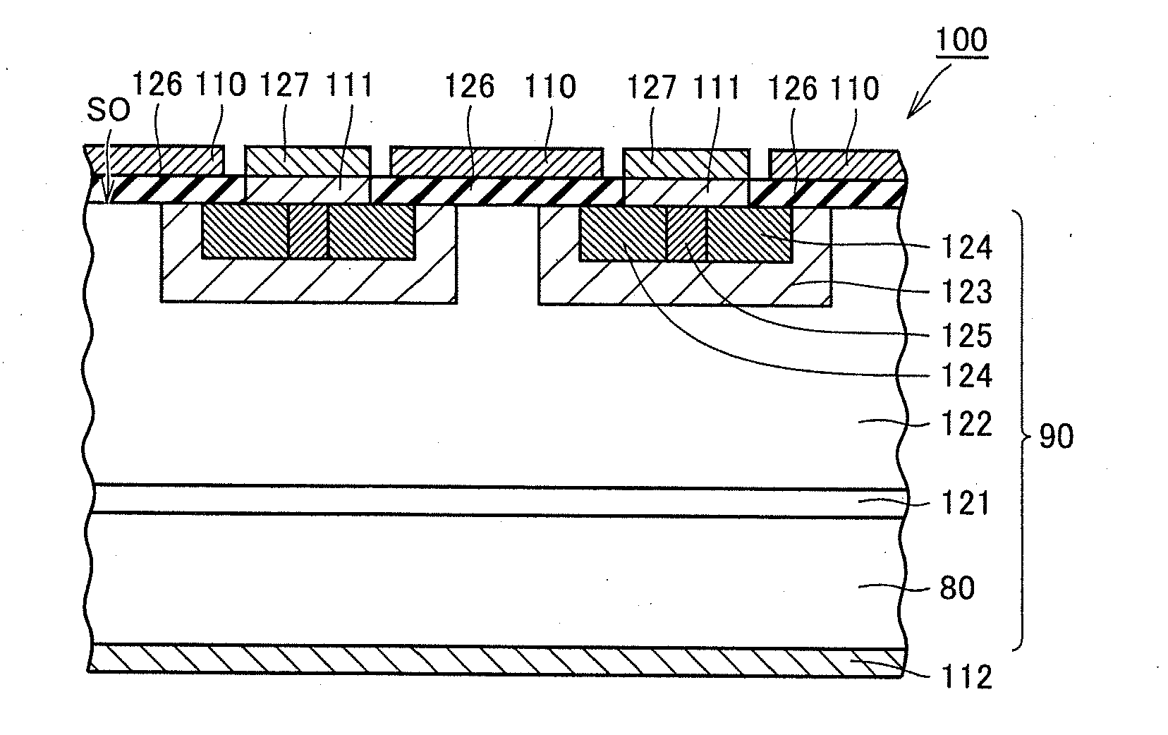
Figure 1 
Figure 2 
Figure 3
Abstract
Description
BACKGROUND OF THE INVENTION
[0001] 1. Field of the Invention
[0002] The present invention relates to a method for manufacturing a silicon carbide semiconductor device and particularly to a method having a step of implanting impurity ions.
[0003] 2. Description of the Background Art
[0004] A semiconductor device (a silicon carbide semiconductor device) including a silicon carbide (SiC) substrate has recently been developed. In a method of manufacturing a semiconductor device, an impurity region should selectively be formed in a silicon carbide substrate. Therefore, a mask is formed for restricting a region into which ions are to be implanted, in implanting ions into the silicon carbide substrate. In addition, a film for adjusting a depth of implantation may be formed on the silicon carbide substrate.
[0005] For example, according to Japanese Patent Laying-Open No. 2009-177102, an ion implantation mask composed of SiO2 is formed on a surface of an SiC substrate. In addition, after the mask is f...
Examples
first embodiment
[0054]As shown in FIG. 1, a silicon carbide semiconductor device in the present embodiment is a MOSFET 100, and it is specifically a vertical DiMOSFET (Double Implanted MOSFET). MOSFET 100 has an epitaxial substrate 90, an oxide film 126, a source electrode 111, an upper source electrode 127, a gate electrode 110, and a drain electrode 112. Epitaxial substrate 90 has a single crystal substrate 80, a buffer layer 121, a breakdown voltage holding layer 122, a p region 123, an n+ region 124, and a p+ region 125. A two-dimensional shape (a shape when viewed from above in FIG. 1) of MOSFET 100 is for example, a rectangle or a square having a side of a length not shorter than 2 mm.
[0055]Single crystal substrate 80 and buffer layer 121 each have an n conductivity type. Single crystal substrate 80 is preferably composed of silicon carbide.
[0056]Concentration of an n-type conductive impurity in buffer layer 121 is, for example, 5×1017 cm−3. In addition, buffer layer 121 has a thickness, for ...
second embodiment
[0093]As shown in FIG. 21, in the present embodiment, after coating film 50 is formed and before ion implantation by using ion beams J1 is carried out, a blocking film 61a (a first blocking film) made of a material higher in capability of blocking ion beams than the material for coating film 50 is formed. In particular, in the present embodiment, blocking film 61a is formed after opening P1 is formed. A material for blocking film 61a may be the same as the material for mask layer 31, and it is, for example, silicon oxide.
[0094]Since the construction other than the above is substantially the same as in the first embodiment described above, the same or corresponding elements have the same reference characters allotted and description thereof will not be repeated.
[0095]According to the present embodiment, after ion beams J1 (FIG. 21) pass through not only coating film 50 but also blocking film 61a, they reach epitaxial substrate 90. Thus, a shallow position in implantation profile PF (...
third embodiment
[0097]As shown in FIG. 22, in the present embodiment, a blocking film 61b (a first blocking film) is formed before mask layer 31 is formed.
[0098]Since the construction other than the above is substantially the same as in the second embodiment described above, the same or corresponding elements have the same reference characters allotted and description thereof will not be repeated. According to the present embodiment, after ion beams J1 (FIG. 22) pass through not only coating film 50 but also blocking film 61b, they reach epitaxial substrate 90. Thus, a shallow position in implantation profile PF (FIG. 20) (a portion close to the origin on the abscissa) is occupied by a portion other than epitaxial substrate 90 across a wider range. Therefore, a concentration profile formed from surface SO of epitaxial substrate 90 to a portion in the vicinity thereof can be a portion of implantation profile PF, excluding by a wider range a portion at a shallow position. More specifically, a concent...