
Normally off gallium nitride field effect transistors (FET)
a field effect transistor and gallium nitride technology, applied in the field of semiconductor device configuration and manufacturing methods, can solve the problems of more complicated devices, device not suitable for those applications, and additional power consumption, and achieve the effects of improving device configuration, simple and convenient manufacturing and operating processes, and improving device configuration
Patent Information
- Authority / Receiving Office
- US · United States
- Patent Type
- Applications(United States)
- Current Assignee / Owner
- Publication Date
- 2014-06-26
Smart Images
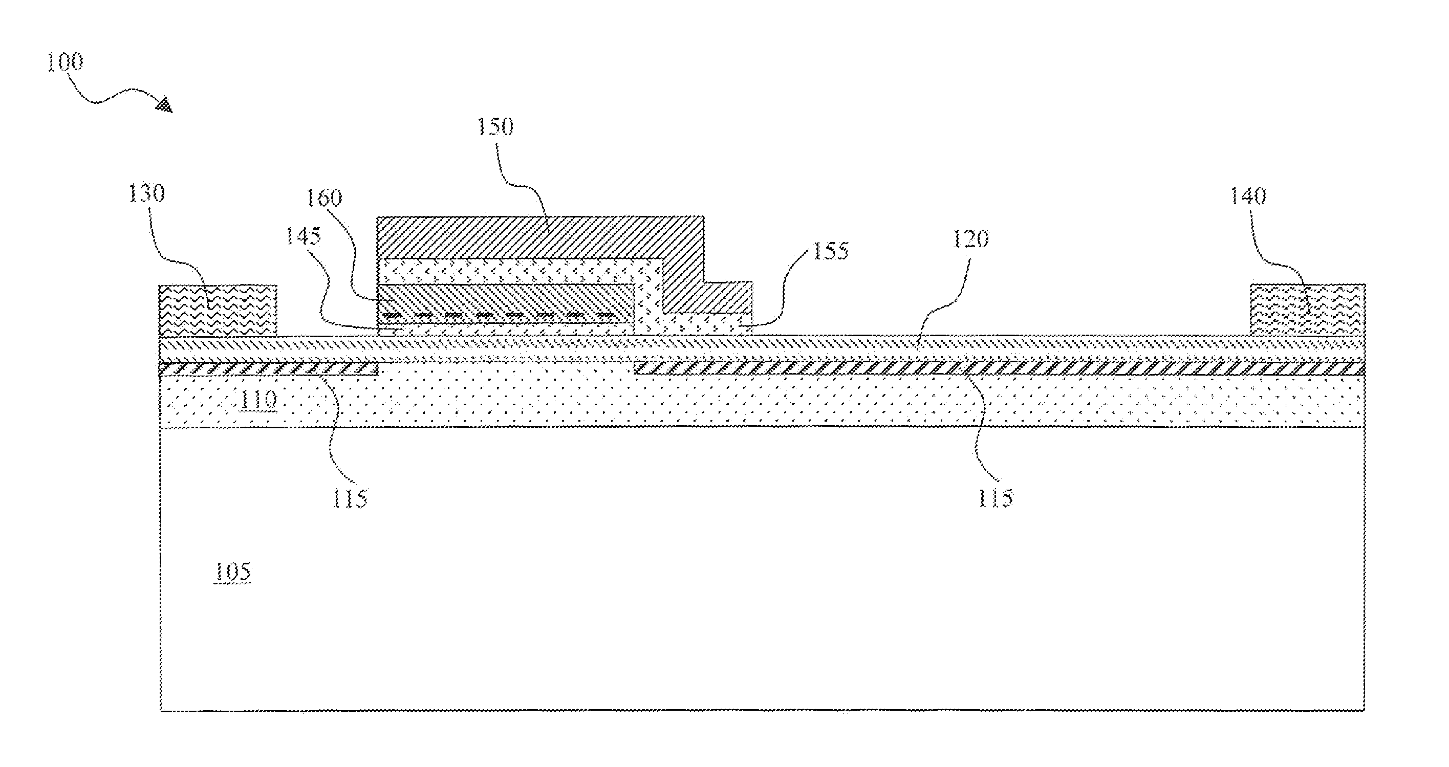
Figure 1 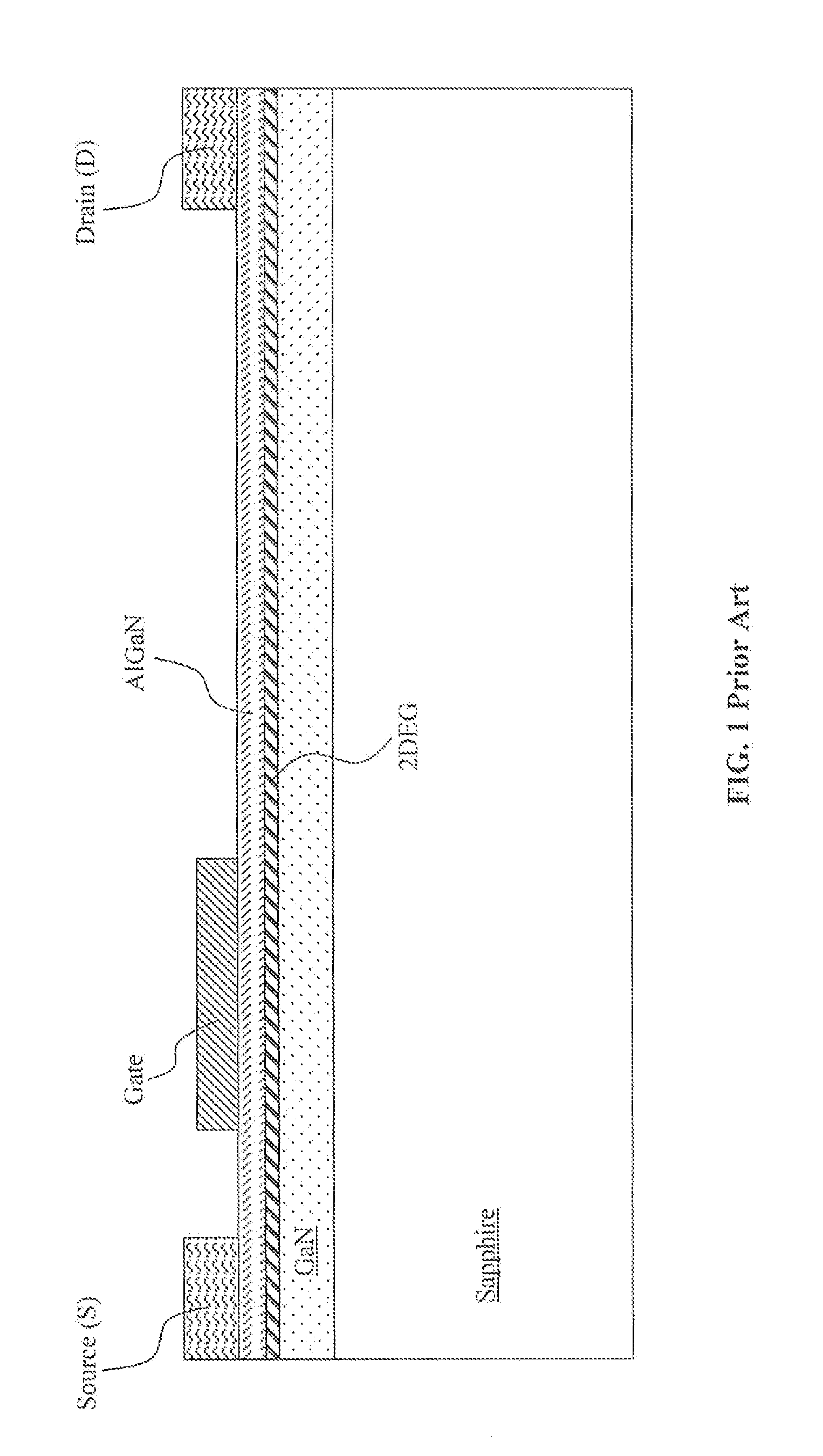
Figure 2 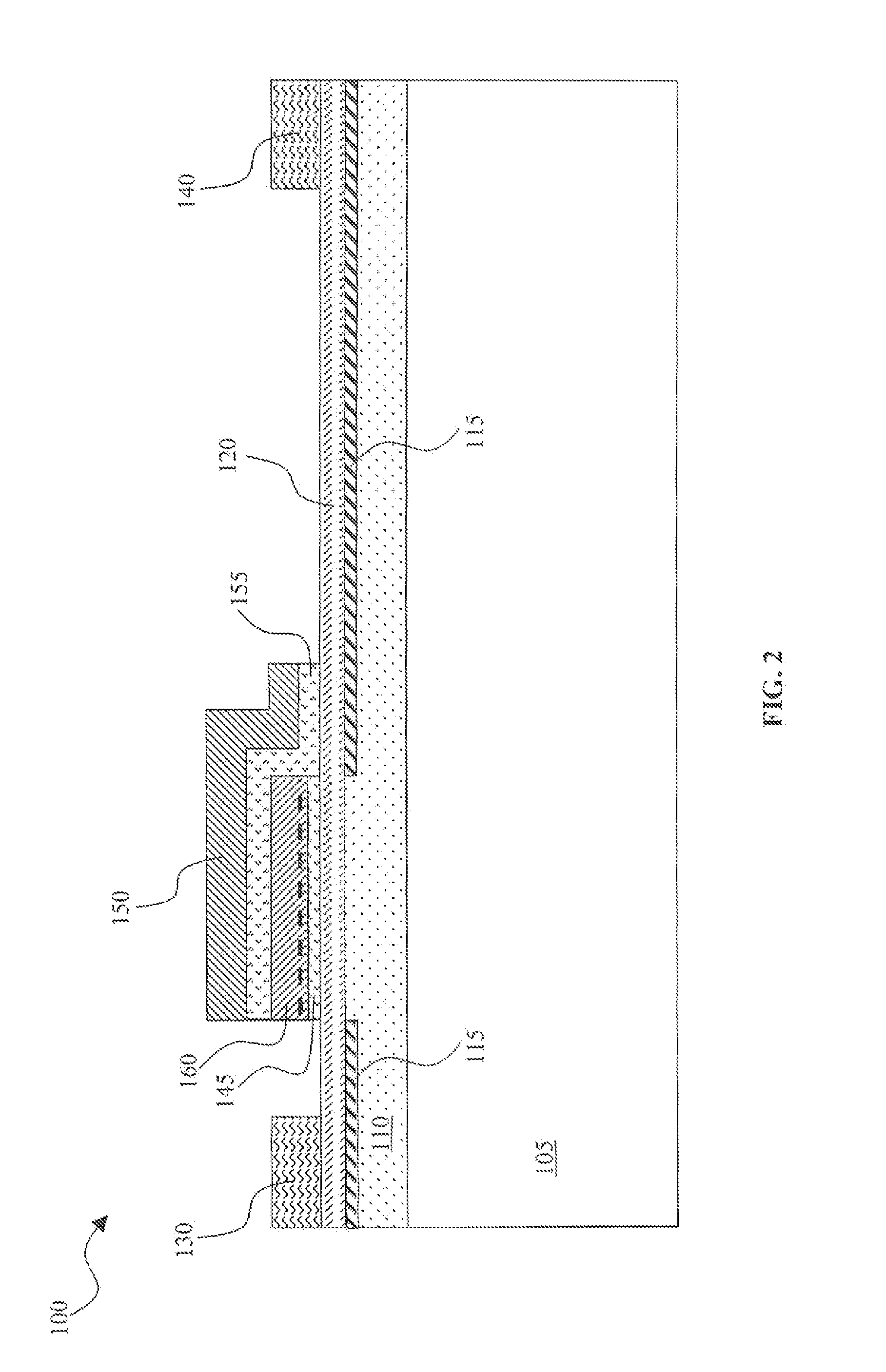
Figure 3
Abstract
Description
[0001] This application is a Continuous Application, and claims priority of a pending application Ser. No. 12 / 589,945 filed on Oct. 30, 2009 by the common inventors of this Application. The benefit of the filing dates are hereby claimed under Title 35 of the United States Code. The disclosures of applications Ser. No. 12 / 589,945 are hereby incorporated by reference,BACKGROUND OF THE INVENTION
[0002] 1. Field of the Invention
[0003] The invention relates generally to the configurations and methods of manufacturing the semiconductor devices. More particularly, this invention relates to a gallium nitride (GaN)-based field effect transistor implemented with new device configurations and manufacturing methods for a normally-off GaN-based field effect transistor that has an extremely small ON resistance in conducting a large amount of electric current.
[0004] 2. Description of the Prior Art
[0005] Conventional methods of configuring, and manufacturing a gallium nitride (GaN) based field effect tr...
Examples
Embodiment Construction
[0022]Referring to FIG. 2 for a cross sectional view of a heterostructure field effect transistor (HFET) semiconductor power device 100 of this invention. The HEFT semiconductor power device 100 comprises an AlGaN layer 120 epitaxial grown on top of gallium nitride (GaN) layer 110 thus forming a AlGaN / GaN hetero-junction with a two-dimensional electron gas (2DEG) 115 located at the interface. The AlGalN / GaN hetero-junction structure is supported on a sapphire substrate 105. A source electrode 130 and a drain 140 are disposed on two opposite sides of a gate electrode 150 to control the current flow through the 2DEG layer 115. The gate electrode 150 is insulated from the N-doped AlGaN layer 120 with a thicker gate oxide layer 155. In order to configure the HFET power device as a normally off device, a floating gate 160 is formed beneath at least a portion of the gate oxide layer 155. The floating gate 160 is insulated from the AlGaN layer 120 with a thin oxide layer 145, and from the ...