
Method for forming fin-shaped structure
Patent Information
- Authority / Receiving Office
- US · United States
- Current Assignee / Owner
- Publication Date
- 2014-08-21
Smart Images
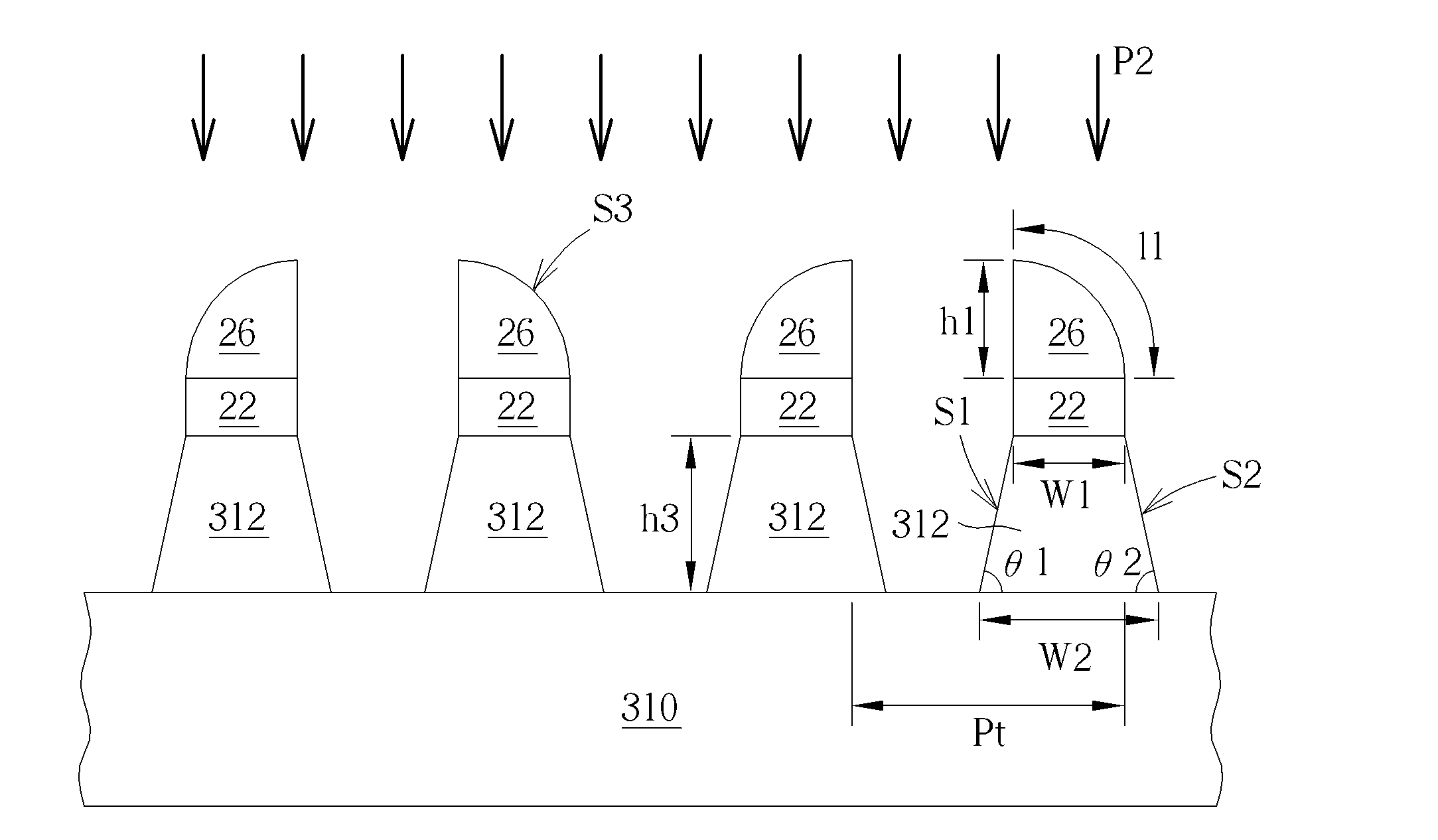
Figure 1 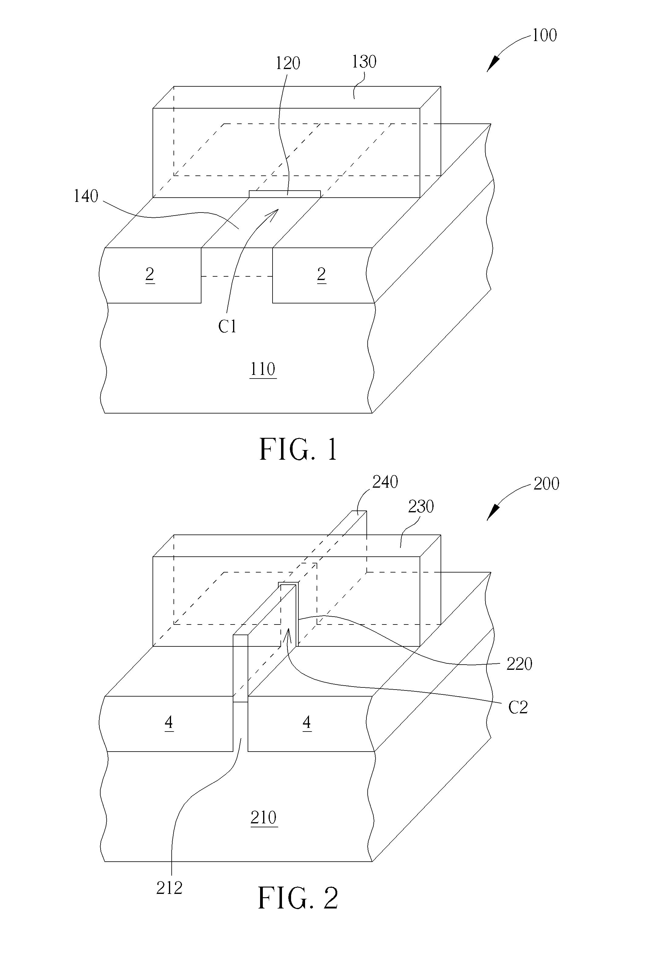
Figure 2 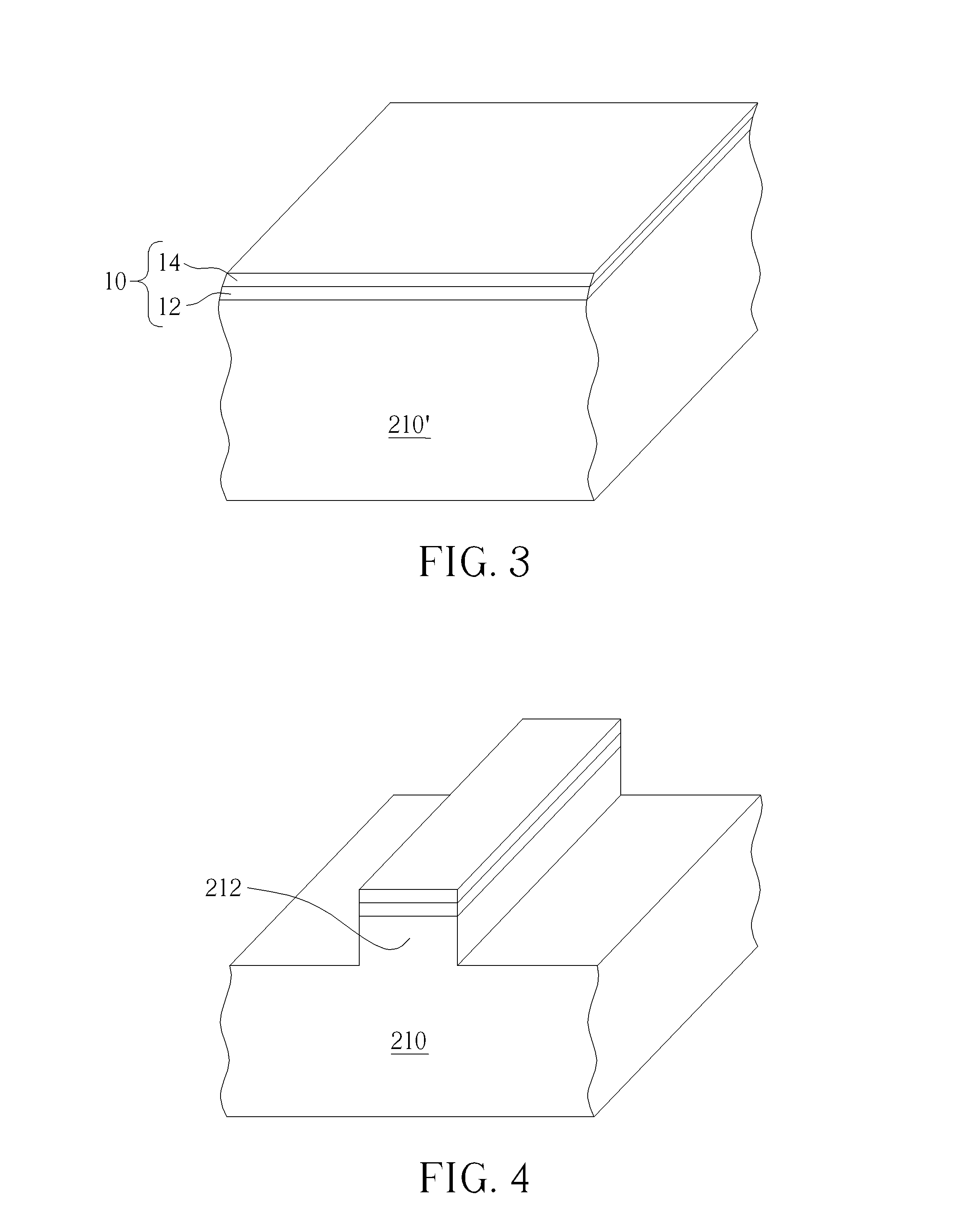
Figure 3
Abstract
Description
BACKGROUND OF THE INVENTION
[0001] 1. Field of the Invention
[0002] The present invention relates generally to a method for forming a fin-shaped structure, and more specifically to a method for forming a fin-shaped structure having a taper profile.
[0003] 2. Description of the Prior Art
[0004] With the increasing miniaturization of semiconductor devices, various multi-gate MOSFET devices have been developed. The multi-gate MOSFETs are advantageous for the following reasons. First, the manufacturing processes of the multi-gate MOSFET devices can be integrated into traditional logic device processes, and thus are more compatible. In addition, since the three-dimensional structure of a multi-gate MOSFET increases the overlapping area between the gate and the substrate, its channel region is controlled more effectively. This therefore reduces drain-induced barrier lowering (DIBL) effect and short channel effect. Moreover, the channel region is longer for a similar gate length. Therefore, the cu...
Examples
first embodiment
[0015]FIG. 1 schematically depicts a three-dimensional diagram of a planar transistor according to the present invention. As shown in FIG. 1, a planar transistor 100 includes a substrate 110, at least an isolation structure 2, a gate dielectric layer 120, an electrode 130 and a source / drain region 140. The substrate 110 may be a semiconductor substrate such as a silicon substrate, a silicon containing substrate such as a silicon carbide substrate, a III-V group-on-silicon (such as GaN-on-silicon) substrate, a graphene-on-silicon substrate, a silicon-on-insulator (SOI) substrate or an epitaxial layer containing a substrate such as a P-type substrate with a 2.5 μm P-type epitaxial layer. The isolation structure 2 is located in the substrate 110, wherein the isolation structure 2 is used to isolate each transistor formed on the substrate 110. The isolation structure 2 may be a shallow trench isolation (STI) structure, which may be formed through a shallow trench isolation (STI) process...
second embodiment
[0020]FIG. 2 schematically depicts a three-dimensional diagram of a multi-gate MOSFET according to the present invention. In FIG. 2 one example of a multi-gate MOSFET—a tri-gate MOSFET—is shown. A tri-gate MOSFET 200 may include a substrate 210, a fin-shaped structure 212, at least an isolation structure 4, a gate dielectric layer 220, an electrode 230 and a source / drain region 240.
[0021]The fin-shaped structure 212 is located on the substrate 210. Generally, the fin-shaped structure 212 and the substrate 210 form one piece only, but the fin-shaped structure 212 may be additionally formed on the substrate 210, depending upon the needs. The substrate 210 may be a semiconductor substrate such as a silicon substrate, a silicon containing substrate such as a silicon carbide substrate, a III-V group-on-silicon (such as GaN-on-silicon) substrate, a graphene-on-silicon substrate, a silicon-on-insulator (SOI) substrate or an epitaxial layer containing substrate such as a P-type substrate wi...
third embodiment
[0032]FIGS. 5-10 schematically depict cross-sectional views of a method for forming a fin-shaped structure according to the present invention. As shown in FIG. 5, a substrate 310 is provided, wherein the substrate 310 may be a semiconductor substrate such as a silicon substrate, a silicon containing substrate such as a silicon carbide substrate, a III-V group-on-silicon (such as GaN-on-silicon) substrate, a graphene-on-silicon substrate, a silicon-on-insulator (SOI) substrate or an epitaxial layer containing substrate such as a P-type substrate with a 2.5 μm P-type epitaxial layer. A pad layer 22 is formed on the substrate 310, wherein the pad layer 22 may include an oxide layer, but it is not limited thereto. A sacrificial pattern material 24′ is formed to entirely cover the pad layer 22. As shown in FIG. 6, the sacrificial pattern material 24′ is patterned to form a sacrificial pattern 24. In this embodiment, the sacrificial pattern material 24′ is polysilicon, and the sacrificial...