
Light emitting device
Patent Information
- Authority / Receiving Office
- US · United States
- Current Assignee / Owner
- Publication Date
- 2016-04-28
Smart Images
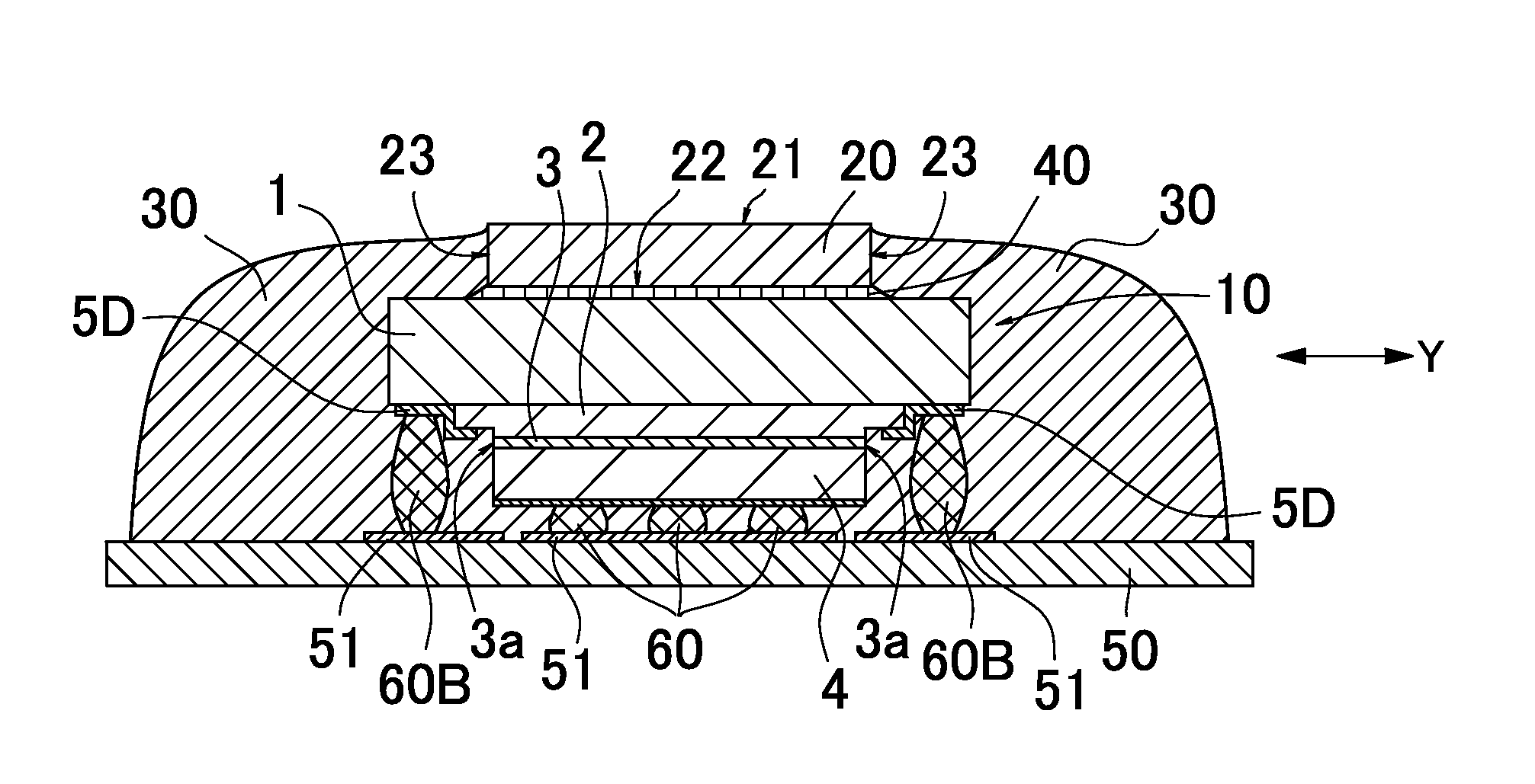
Figure 1 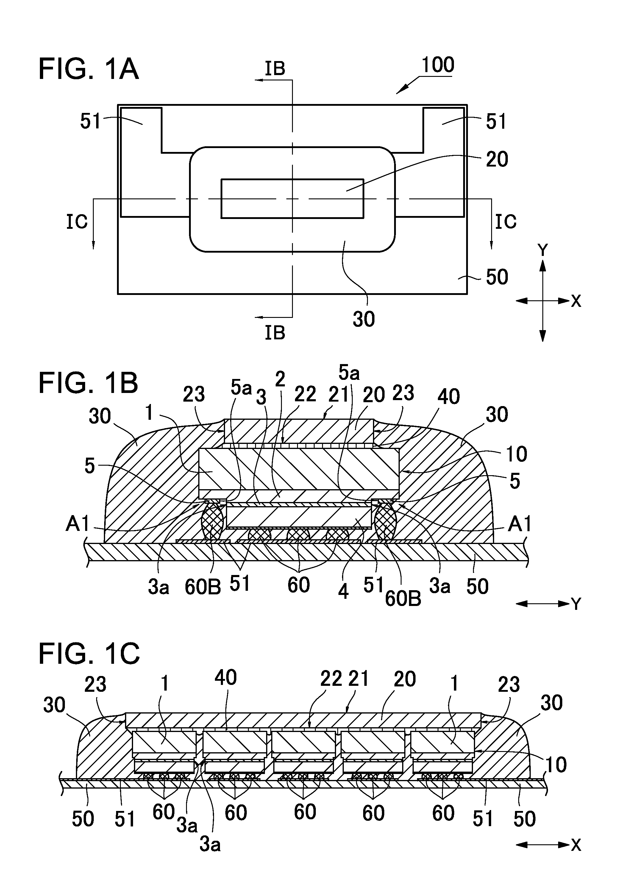
Figure 2 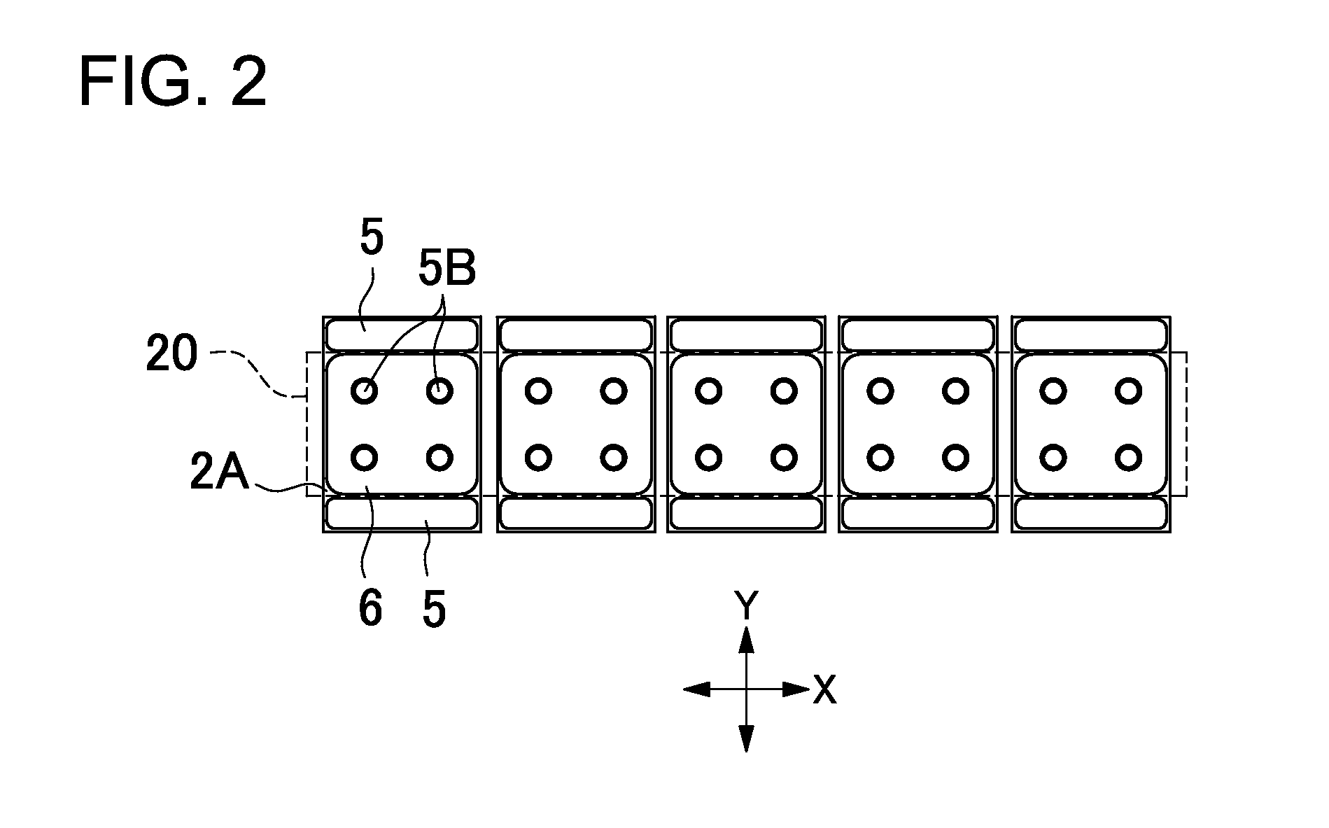
Figure 3
Abstract
Description
CROSS-REFERENCE TO RELATED APPLICATIONS
[0001] The present application claims priority under 35 U.S.C. 119 to Japanese Patent Application No. 2014-219242 filed Oct. 28, 2014 and Japanese Patent Application No. 2015-208605 filed Oct. 23, 2015. The contents of that application are incorporated herein by reference in their entirety.BACKGROUND OF THE INVENTION
[0002] 1. Field of the Invention
[0003] The present disclosure relates to a light emitting device.
[0004] 2. Description of the Related Art
[0005] Light emitting elements such as light emitting diodes (LEDs) and laser diodes (LDs) are widely used in a variety of light source applications (e.g. backlight of liquid crystal display), general lightings, traffic signals, and wide-screen displays, or the like. In addition, recent advances of increase in light output have made light emitting elements a viable option for automobile headlight applications.
[0006] Currently, light emitting devices for applications required high light output, a pluralit...
Examples
first embodiment
[0022]FIGS. 1A-3B show a light emitting device 100 according to the first embodiment of the present invention. FIG. 1A is a schematic plan view, FIG. 1B is a schematic cross-section through the line IB-IB in FIG. 1A, FIG. 1C is a schematic cross-section through the line IC-IC in FIG. 1A, FIG. 2 is a schematic plan view of light emitting elements 10 arranged in a row in a first direction X of the light emitting device 100, FIG. 3A is a schematic plan view of a light emitting element 10, and FIG. 3B is a schematic cross-section through the line IIIB-IIIB in FIG. 3A. As shown in FIGS. 1A-3B, the light emitting device 100 according to the first embodiment is provided with a mounting board 50, a plurality of light emitting elements 10 arranged on the mounting board 50 with gaps in a row in the first direction X, wavelength-conversion member 20 disposed on the light extraction surface 21 side of the light emitting elements 10 so as to cover the tops of the light emitting elements 10 and t...
second embodiment
[0050]Light emitting device according to the second embodiment are shown in the schematic plan view of FIG. 4. Other than light emitting element 10 structure, component parts of a light emitting device that includes the light emitting elements 10 shown in FIG. 4 are essentially the same as that of the above described first embodiment. Accordingly, similar components are indicated by the same reference numbers and for expediency their description is not repeated.
[0051]As shown in FIG. 4, light emitting elements 10B at both ends of the row of light emitting elements 10 aligned in the first direction X have extended areas A3 that extend beyond the ends of the wavelength-conversion member 20 in the first direction X as shown in dashed line in FIG. 4. The extended areas A3 are parts of the exposed area 2A which exposes n-type semiconductor layer 2, and the extended areas A3 are formed in a manner continuous with the n-type semiconductor layers 2 of the light emitting elements 10B. In a c...
third embodiment
[0052]Light emitting devoice according to the third embodiment are shown in FIGS. 5A-5B. FIG. 5A is a schematic plan view of the light emitting element 10, FIG. 5B is a schematic cross-section of the light emitting device having the light emitting element 10 shown in FIG. 5A. It should be noted that FIG. 5B includes schematic cross-section of the light emitting element 10 through the line A-A in FIG. 5A. Other than light emitting element 10 structure shown in FIGS. 5A-5B, component parts of light emitting devices according to the third embodiment are essentially the same as above described in the first embodiment. Accordingly, similar components are indicated by the same reference numbers and for expediency their description is not repeated. In addition, hatched areas in FIG. 5A indicate exposed area 2A.
[0053]As shown in FIG. 5B, light-transmissive substrate 1 extends in the second direction Y beyond exposed n-type semiconductor layer 2 in end regions A1′, and n-side electrodes 5D a...