
Flexible electronic device having adhesive function and method for manufacturing same
a flexible electronic device and function technology, applied in the direction of sustainable manufacturing/processing, transistors, final product manufacturing, etc., can solve the problems of increasing the number of manufacturing processes, device may still break, and not structurally compatible with existing two-dimensional planar devices, so as to achieve the effect of maintaining performance over a long period of time and minimizing the breakage of electronic devices
Patent Information
- Authority / Receiving Office
- US · United States
- Patent Type
- Applications(United States)
- Current Assignee / Owner
- Publication Date
- 2017-01-26
Smart Images
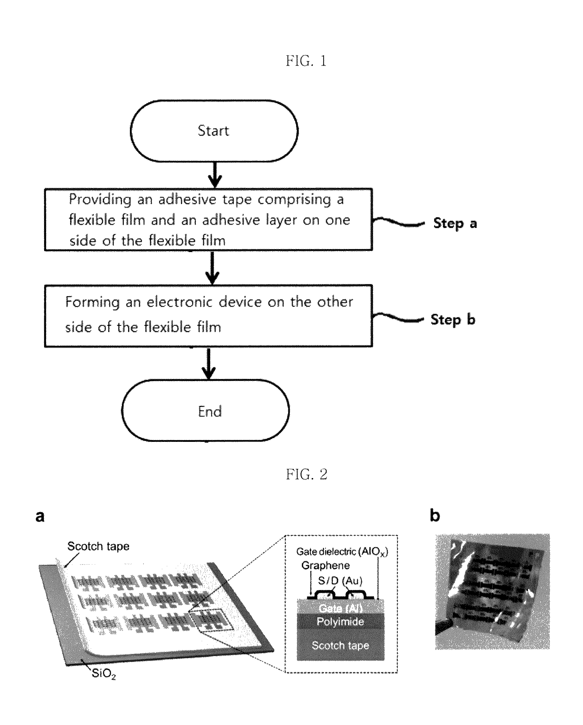
Figure 1 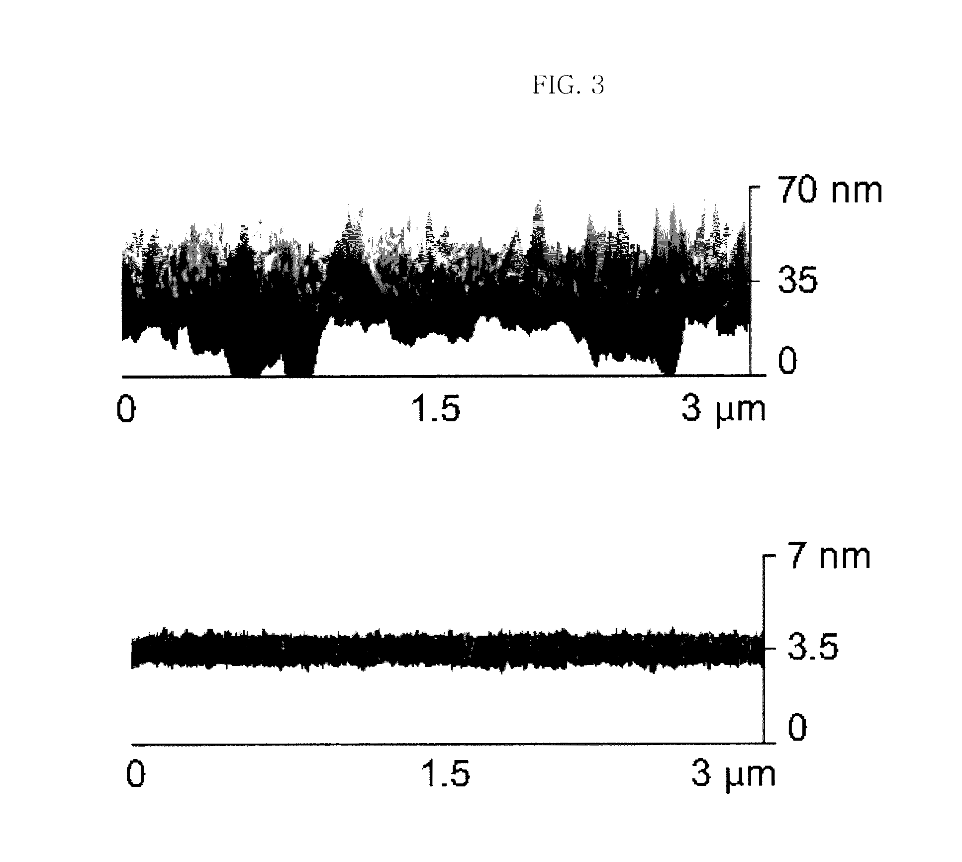
Figure 2 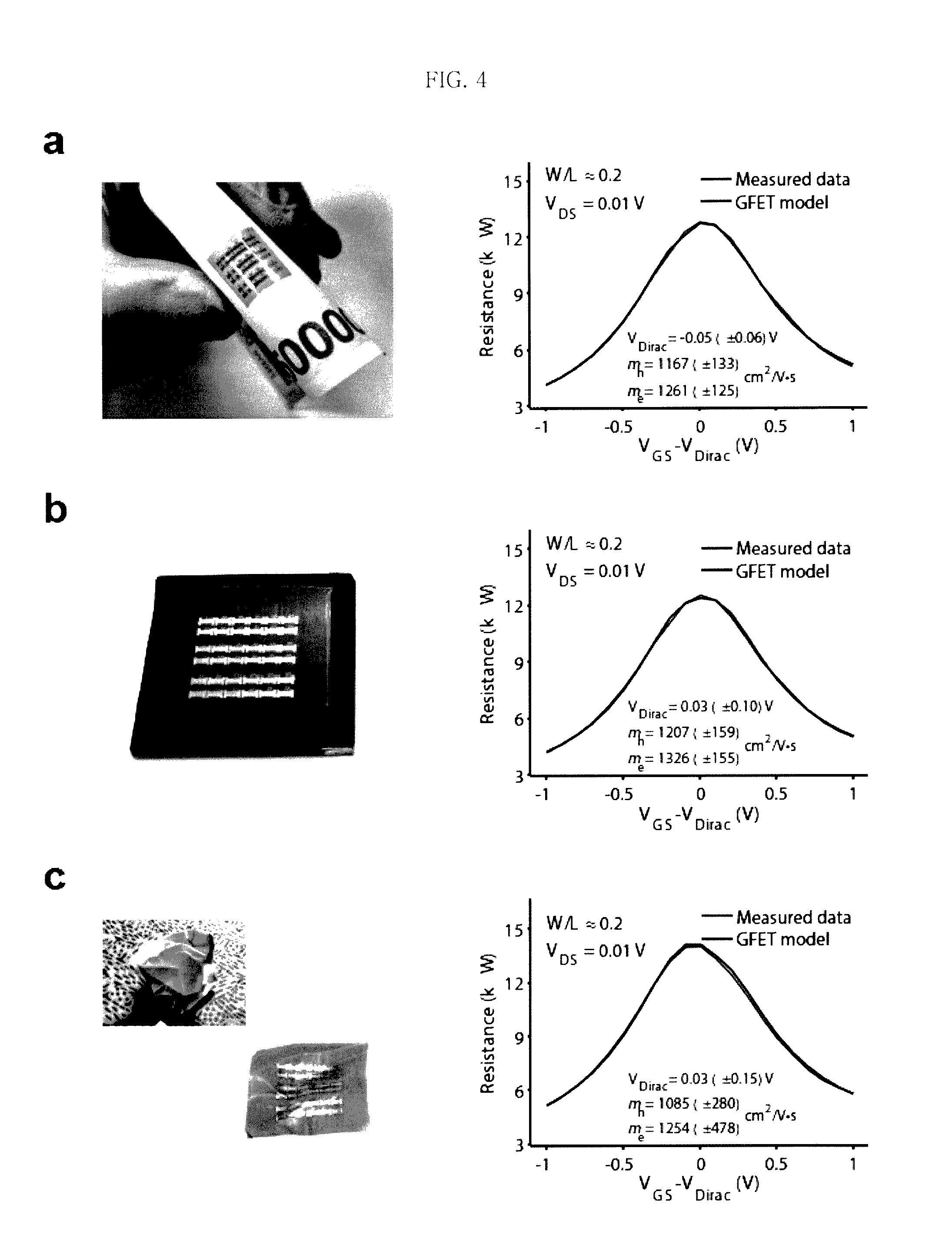
Figure 3
Abstract
Description
[0001] The present application claims the priority benefit of Korean Patent Application No. 10-2015-0102689 filed Jul. 20, 2015, which is hereby incorporated by reference.BACKGROUND OF THE INVENTION
[0002] 1. Field of the Invention
[0003] The present invention relates to a flexible electronic device having an adhesive function and a method of manufacturing the same, and to a technology of forming a flexible electronic device on an adhesive tape that includes an adhesive layer so as to manufacture a flexible electronic device having an adhesive function.
[0004] 2. Description of the Related Art
[0005] It is expected that flexible electronic devices will be an important technological component in future industries. For example, a thin film transistor embodied on a plastic substrate may be used to drive a bendable liquid crystal display device, electronic paper, which has attracted great attention recently, or an organic light emitting device. In particular, electronic paper, which has been dev...
Examples
example
Example 1
[0085]Scotch tape was prepared as the adhesive tape including polytetrafluoroethylene (PTFE) as the flexible film and the silicon-based adhesive as the adhesive layer (3M™, 5480, PTFE thickness of 50 μm, and silicon-based adhesive thickness of 44 μm). The Scotch tape was attached to the silicon wafer.
[0086]Next, the polyimide solution (VTEC™, P1-1388) was applied on the tape attached to the silicon wafer using spin coating at 3000 rpm for 30 sec, and sequentially baked at 60° C. and 150° C. for 10 min to form the polyimide surface reforming layer.
[0087]Next, the aluminum layer (30 nm), as the gate electrode, was deposited on the surface reforming layer using heat in the thermal deposition apparatus using the shadow mask.
[0088]The aluminum layer was then oxidized in the oxygen plasma chamber under the condition of RF power (radio frequency power) of 250 W for 7 min to form the gate insulating layer on the surface of the aluminum layer. Oxygen pressure was maintained as low a...
example 2
[0092]The graphene field-effect transistor was manufactured using the same method and condition as Example 1, except that the pressure of the oxygen plasma chamber was 50 mTorr rather than 12 mTorr when the gate insulating layer was formed.
example 3
[0093]The graphene field-effect transistor was manufactured using the same method and condition as Example 1, except that the pressure of the oxygen plasma chamber was 100 mTorr rather than 12 mTorr when the gate insulating layer was formed.