
Active matrix device and method of driving
a technology of active matrix and driving method, applied in the field of active matrix array, can solve the problem of not disclosing any circuit embodiment, and achieve the effect of improving linearity
Patent Information
- Authority / Receiving Office
- US · United States
- Patent Type
- Applications(United States)
- Current Assignee / Owner
- Publication Date
- 2017-03-16
Smart Images
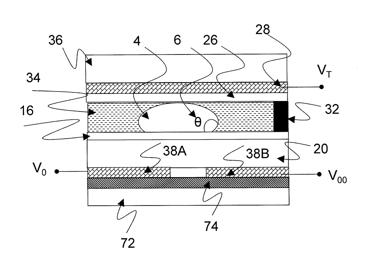
Figure 1 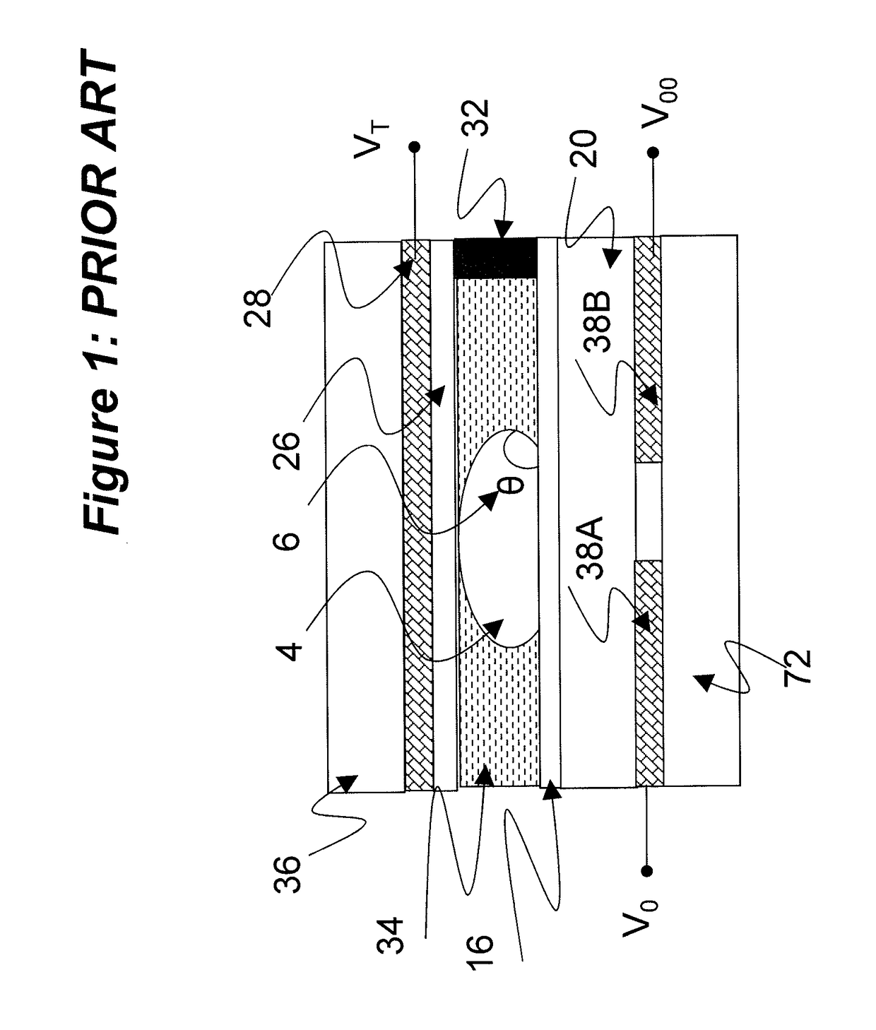
Figure 2 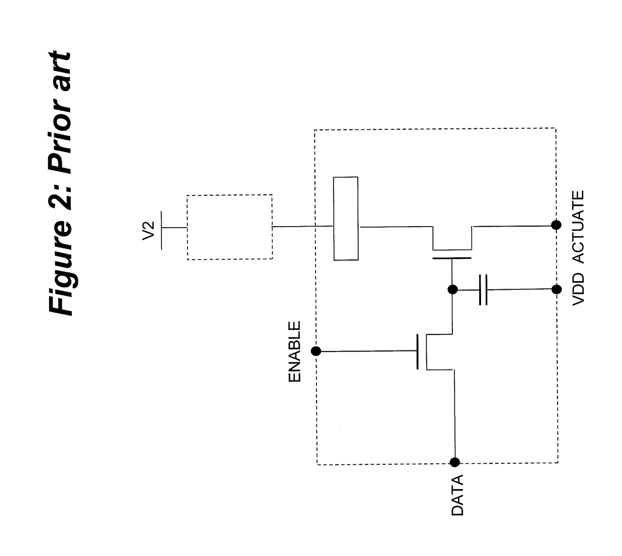
Figure 3
Abstract
Description
TECHNICAL FIELD
[0001] The present invention relates to active matrix arrays and elements thereof. In a particular aspect, the present invention relates to digital microfluidics, and more specifically to Active Matrix Electro-wetting-On-Dielectric (AM-EWOD), and further relates to methods of driving such a device.BACKGROUND ART
[0002] Electro-wetting on dielectric (EWOD) is a well known technique for manipulating droplets of fluid by application of an electric field. Active Matrix EWOD (AM-EWOD) refers to implementation of EWOD in an active matrix array incorporating transistors, for example by using thin film transistors (TFTs). It is thus a candidate technology for digital microfluidics for lab-on-a-chip technology. An introduction to the basic principles of the technology can be found in “Digital microfluidics: is a true lab-on-a-chip possible?”, R. B. Fair, Microfluid Nanofluid (2007) 3:245-281).
[0003] FIG. 1 shows a part of a conventional EWOD device in cross section. The device inc...
Examples
first embodiment
[0108]FIG. 9 shows an array element circuit 84 according to the invention. The array element circuit comprises n-type transistors 52, 54, 55, 58 and 62, and capacitors 56 and 60. The element electrode 38, the electrical load circuit 40 present at the element electrode 38 and the reference electrode 28 are shown since they play a role in the operation of the array element circuit 84. The reference electrode may thus be considered to form a part of the array element circuit in the description that follows.
[0109]The array element circuit 84 may typically perform the functions of:[0110](i) Programming data to a memory element contained within the actuator circuit and storing said data. The data to be programmed is typically input by means of an addressing line DATA which may be common to all elements within the same column of the array. The programming of data may typically be controlled by an addressing line ENABLE, which may typically be common to all elements within the same row of t...
case 1
[0118]Droplet Present:
[0119]Where a droplet is present, the dominant electrical coupling of the element electrode 38 is to the reference electrode 28 via the electrical load 40. As previously explained, the electrical load in this case 40A may be approximated by a capacitor whose value is typically of order a pico-Farad. The capacitance of the electrical load 40A will then dominate over other parasitic impedances in the circuit (e.g. that associated with the source-gate capacitance of transistor 54, typically of order femto-Farads). The electrical potential of the element electrode 38 will therefore track the potential of the reference electrode 28, and will thus correspond to a good approximation to the voltage signal V2. This being the case, the potential developed between the element electrode 38 and the reference electrode 28 will approximately be zero. The liquid droplet 4 will therefore be in a non-actuated state, the contact of the liquid droplet 4 with the hydrophobic coatin...
case 2
[0120]No Droplet Present:
[0121]When no liquid droplet 4 is present, the capacitance between the element electrode 38 and the reference electrode 28 is very small as previously explained. The element electrode 38 is therefore now in a high impedance state and its effective potential is only poorly defined, being dependent on the multiple small parasitic capacitances and resistances within the circuit (e.g. the small electrical load 40B capacitance to the reference electrode 28, the small parasitic source to gate capacitance of transistor 54, and the large off resistance of transistor 54). It may therefore be unclear what the effective potential of the element electrode 38 is and therefore the extent to which the element electrode 38 remains effectively non-actuated.
[0122]However, the situation is such that, even with the potential of the element electrode 38 being poorly defined in CASE 2, the device can still support the correct transport of liquid droplets 4. This is because if any...