
Display apparatus
Patent Information
- Authority / Receiving Office
- US · United States
- Current Assignee / Owner
- Publication Date
- 2020-11-12
Smart Images
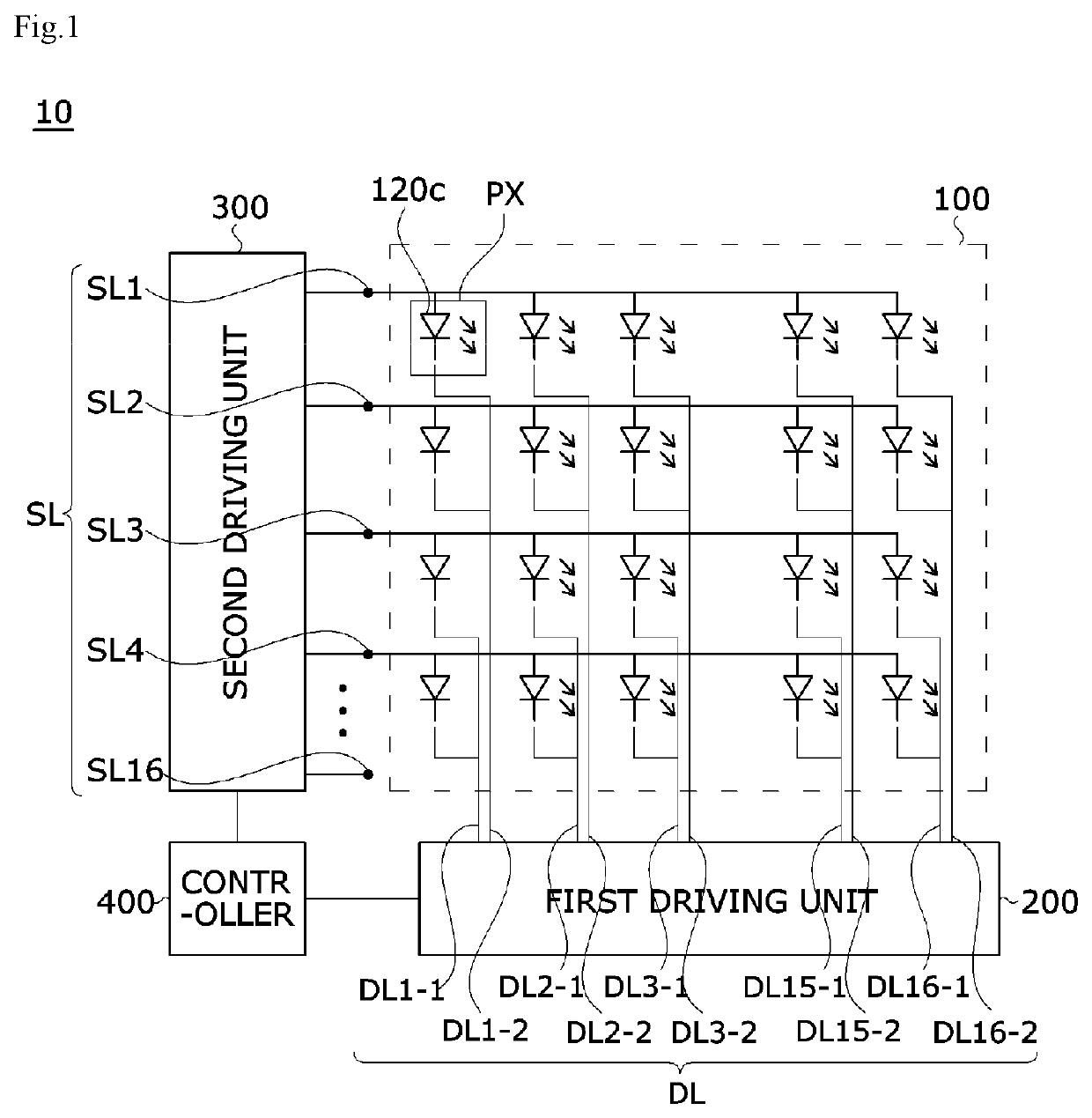
Figure 1 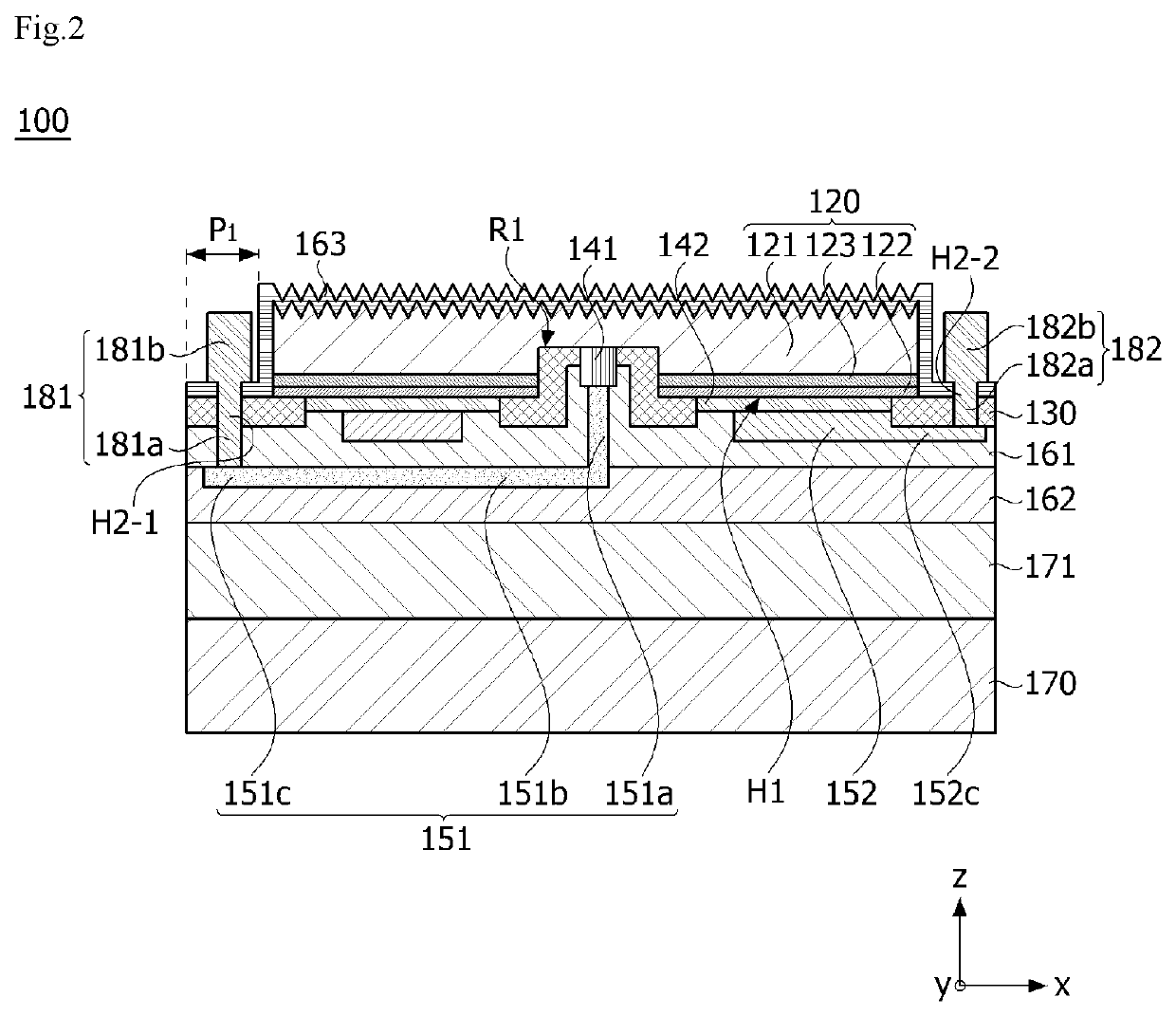
Figure 2 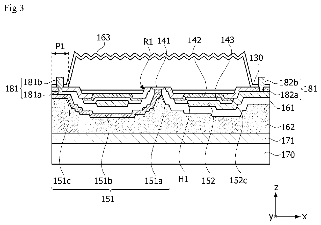
Figure 3
Abstract
Description
TECHNICAL FIELD
[0001] The present invention relates to a display apparatus.BACKGROUND ART
[0002] Semiconductor devices including compounds such as GaN and AlGaN may be variously used as light-emitting devices, light-receiving devices, and various diodes due to many advantages thereof, such as wide and easily adjustable bandgap energy.
[0003] In particular, light-emitting devices, such as light-emitting diodes and laser diodes, which use a III-V group or II-VI group compound semiconductor material, are capable of rendering various colors, such as red, green, and blue, and ultraviolet rays by virtue of the development of thin-film growth technologies and device materials, are capable of producing white light at high efficiency using fluorescent materials or through color mixing, and have advantages such as low power consumption, semi-permanent lifespan, fast response speed, safety, and environmental friendliness as compared with conventional light sources such as fluorescent lamps and inca...
Examples
Embodiment Construction
[0096]While the present invention is open to various modifications and alternative embodiments, specific embodiments thereof will be described and shown by way of example in the accompanying drawings. However, it should be understood that there is no intention to limit the present invention to the particular embodiments disclosed, and, on the contrary, the present invention is to cover all modifications, equivalents, and alternatives falling within the spirit and scope of the present invention.
[0097]It should be understood that, although the terms including ordinal numbers such as first, second, and the like may be used herein to describe various elements, the elements are not limited by the terms. The terms are used only for the purpose of distinguishing one element from another. For example, without departing from the scope of the present invention, a second element could be termed a first element, and similarly a first element could be also termed a second element. The term “and / ...