
Semiconductor package and method of manufacturing the semiconductor package
Patent Information
- Authority / Receiving Office
- US · United States
- Current Assignee / Owner
- Publication Date
- 2022-04-28
Smart Images
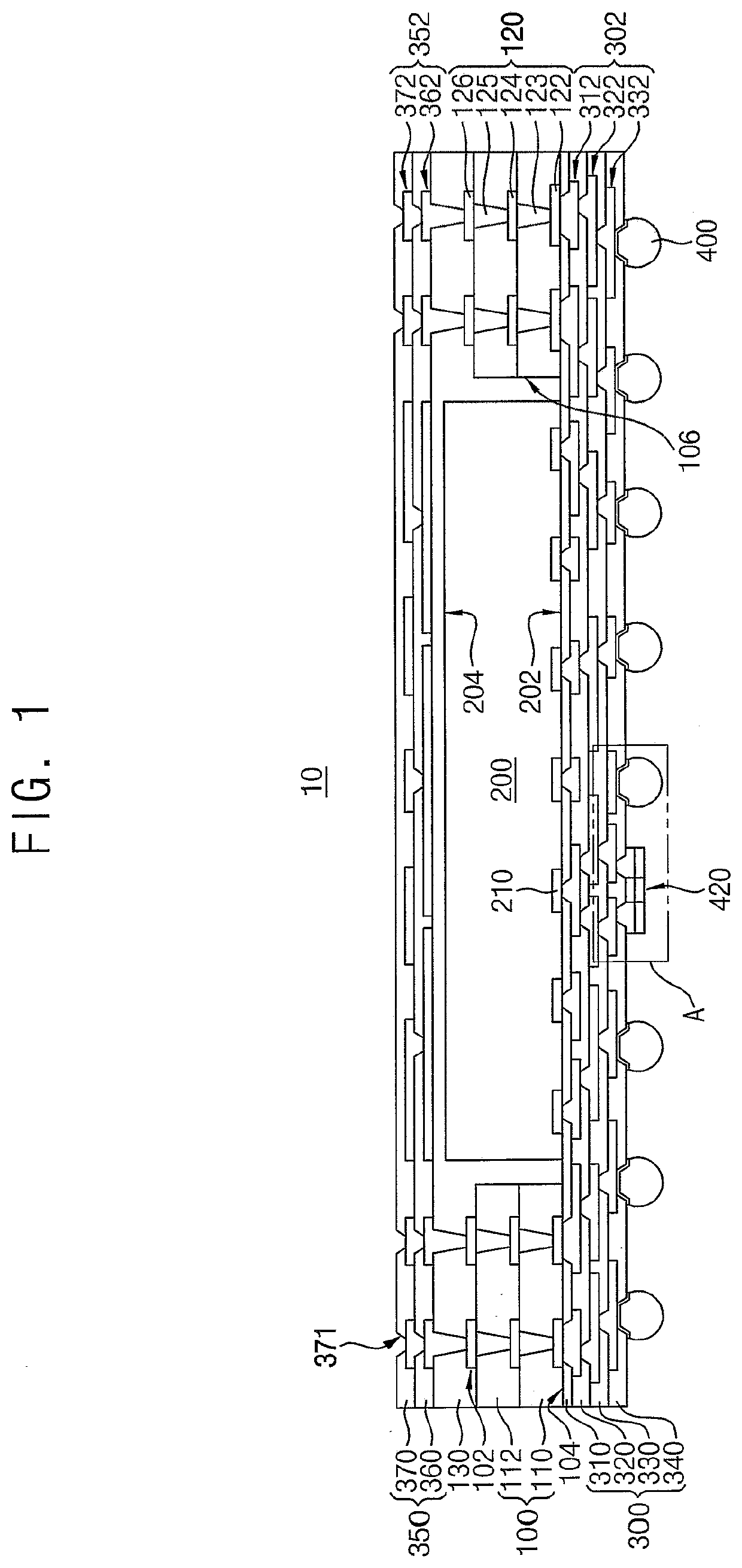
Figure 1 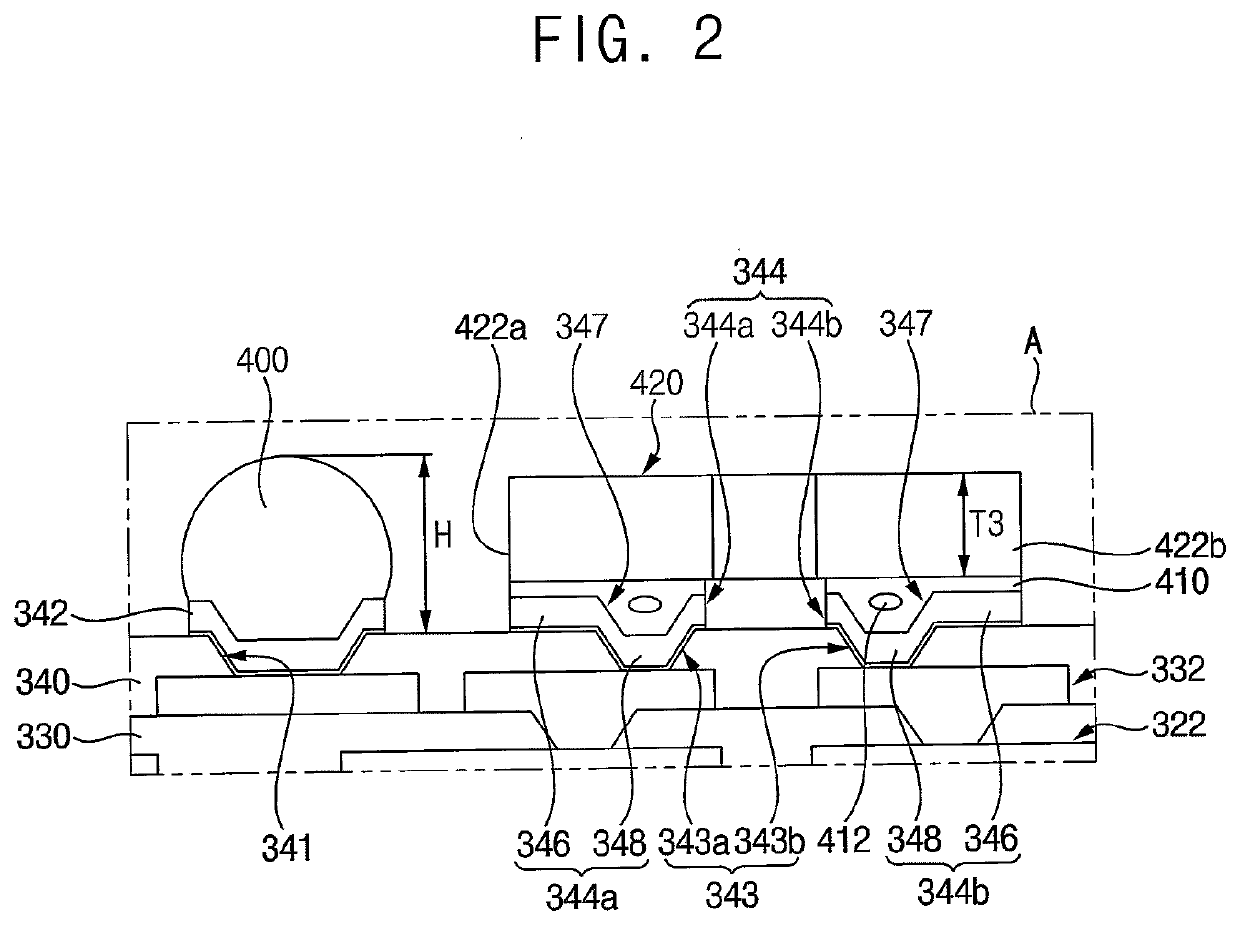
Figure 2 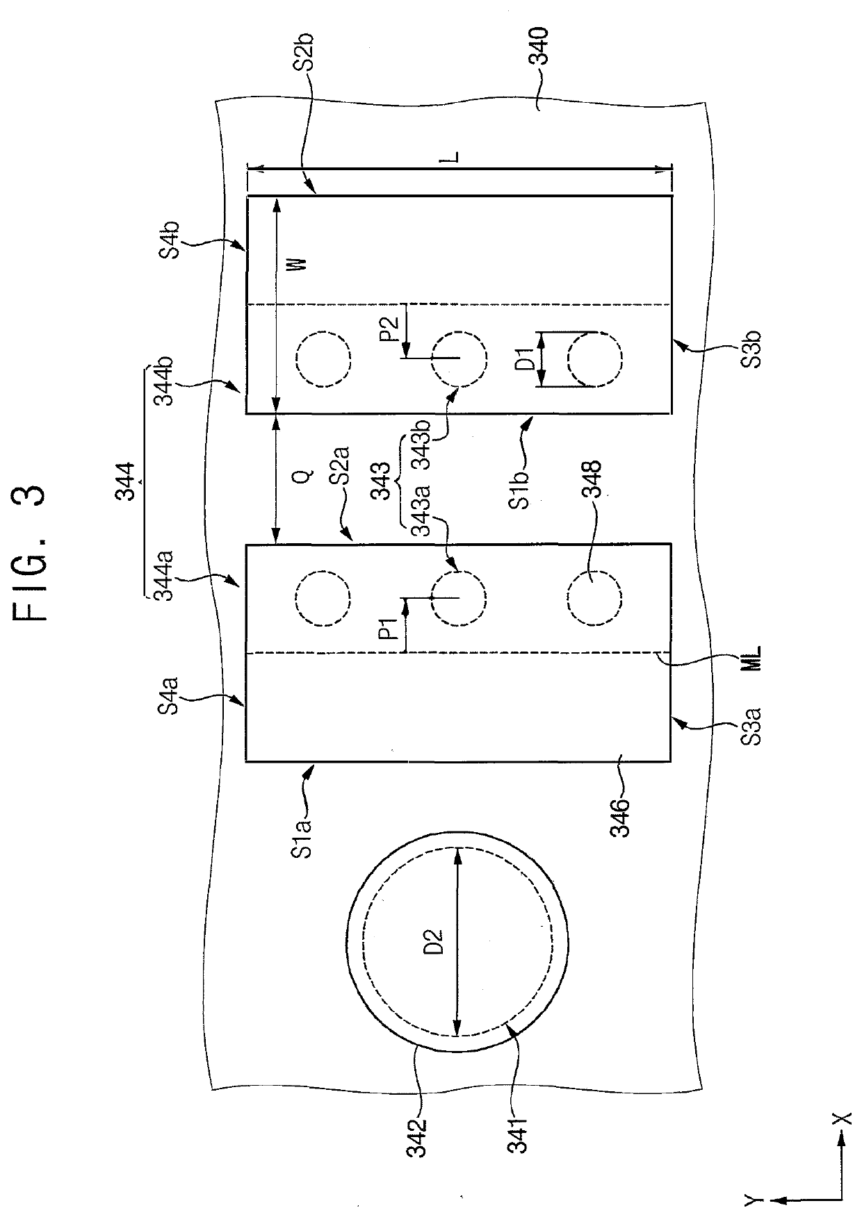
Figure 3
Abstract
Description
PRIORITY STATEMENT
[0001] This application claims priority under 35 U.S.C. § 119 to Korean Patent Application No. 10-2020-0140455, filed on Oct. 27, 2020 in the Korean Intellectual Property Office (KIPO), the contents of which are herein incorporated by reference in their entirety.BACKGROUND1. Field
[0002] Example embodiments relate to semiconductor packages and / or methods of manufacturing the semiconductor package. More particularly, example embodiments relate to semiconductor packages having a passive device and / or methods of manufacturing the same.2. Description of the Related Art
[0003] A fan out package having a relatively thin thickness may include a thin film capacitor capable of implementing a thinner thickness as a passive device. The thin film capacitor may be a decoupling capacitor for an application processor and may be manufactured in the form of a Land-Side Capacitor (LSC). The LSC type capacitor may be mounted via a solder paste. However, during a reflow process for mountin...
Examples
Embodiment Construction
[0025]Hereinafter, some example embodiments will be explained in detail with reference to the accompanying drawings.
[0026]When the terms “about” or “substantially” are used in this specification in connection with a numerical value, it is intended that the associated numerical value includes a manufacturing tolerance (e.g., ±10%) around the stated numerical value. Moreover, when the words “generally” and “substantially” are used in connection with geometric shapes, it is intended that precision of the geometric shape is not required but that latitude for the shape is within the scope of the disclosure. Further, regardless of whether numerical values or shapes are modified as “about” or “substantially,” it will be understood that these values and shapes should be construed as including a manufacturing or operational tolerance (e.g., ±10%) around the stated numerical values or shapes.
[0027]FIG. 1 is a cross-sectional view illustrating a semiconductor package in accordance with some ex...